4283 Group
Note on Power-on reset
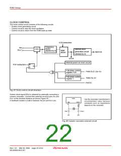
RESET FUNCTION
Under the following condition, the system reset occurs by the
built-in the power-on reset circuit of this product;
The 4283 Group has the power-on reset circuit, though it does
not have RESET pin. System reset is performed automatically
at power-on, and software starts program from address 0 in page
0.
-
when the supply voltage (VDD) rises from 0 V to 2.2 V, within
1 ms.
Also, note that system reset does not occur under the
following conditions;
when the supply voltage (VDD) rises from the voltage higher
than 0V, or
when it takes more than 1 ms for the supply voltage (VDD)
to rise from 0 V to 2.2 V.
In order to make the built-in power-on reset circuit operate
efficiently, set the voltage rising time until VDD= 0 to 2.2 V is
obtained at power-on 1ms or less.
-
-
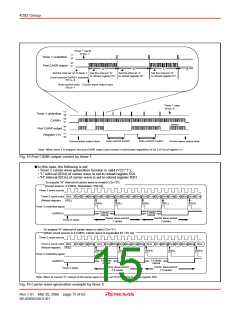
f(XIN)
“H”
Internal reset signal
“L”
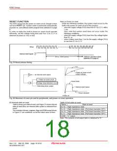
f(XIN) 16384 pulses
Software operation starts
(address 0 in page 0)
Fig. 19 Reset release timing
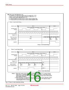
V
DD
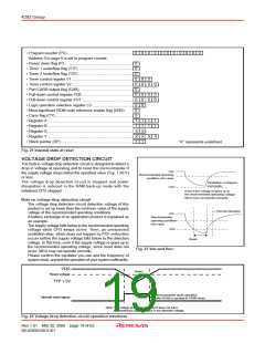
Power-on reset circuit
output voltage
Internal reset signal
Power-on reset circuit
Reset state
Voltage drop detection circuit
Watchdog timer output
Internal reset signal
Reset released
Power-on
Fig. 20 Structure of reset pin and its peripherals, and power-on reset operation
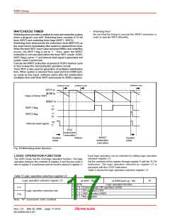
(1) Internal state at reset
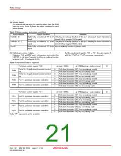
Table 6 Port state at reset
Name
Table 6 shows port state at reset, and Figure 21 shows internal
state at reset (they are retained after system is released from
reset).
The contents of timers, registers, flags and RAM except shown
in Figure 21 are undefined, so set the initial value to them.
State at reset
D0–D3 High impedance state
D4–D7 High impedance state (Pull-down transistor OFF)
G0–G3 High impedance state (Pull-down transistor OFF)
E0, E1
High impedance state (Pull-down transistor OFF)
CARR “L” output
Note: The contents of all output latch is initialized to “0.”
Rev.1.01 Mar 20, 2006 page 18 of 62
REJ03B0109-0101

 RENESAS [ RENESAS TECHNOLOGY CORP ]