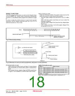
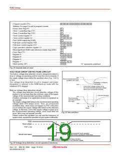
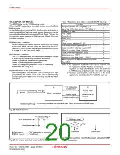
4283 Group
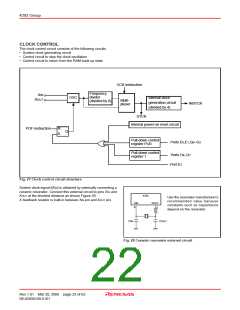
CLOCK CONTROL
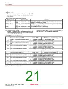
The clock control circuit consists of the following circuits.
• System clock generating circuit
• Control circuit to stop the clock oscillation
• Control circuit to return from the RAM back-up state
CCK instruction
Frequency
XIN
divider
OSC
Internal clock
XOUT
Multi-
plexer
(divided by 8)
generation circuit
(divided by 4)
INSTCK
STCK
Internal power-on reset circuit
POF instruction
R
S
Q
Pull-down control
register PU0
Ports E0,E1,G0–G3
Pull-down control
register 1
Ports D4–D7
Port E2
Fig. 27 Clock control circuit structure
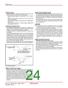
System clock signal f(XIN) is obtained by externally connecting a
ceramic resonator. Connect this external circuit to pins XIN and
XOUT at the shortest distance as shown Figure 28.
4283
Use the resonator manufacturer’s
recommended value bacause
constants such as capacitance
depend on the resonator.
A feedback resistor is built-in between XIN pin and XOUT pin.
XIN
4
XOUT
5
CIN
COUT
Fig. 28 Ceramic resonator external circuit
Rev.1.01 Mar 20, 2006 page 22 of 62
REJ03B0109-0101

 RENESAS [ RENESAS TECHNOLOGY CORP ]