Section 13 Timer Z
Initial
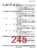
Bit
Bit Name Value
R/W
Description
5
EB1
EA1
ED0
EC0
EB0
EA0
1
1
1
1
1
1
R/W
Master Enable B1
0: FTIOB1 pin output is enabled according to the TPMR,
TFCR, and TIORA_1 settings
1: FTIOB1 pin output is disabled regardless of the TPMR,
TFCR, and TIORA_1 settings (FTIOB1 pin is operated
as an I/O port).
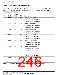
4
3
2
1
0
R/W
R/W
R/W
R/W
R/W
Master Enable A1
0: FTIOA1 pin output is enabled according to the TPMR,
TFCR, and TIORA_1 settings
1: FTIOA1 pin output is disabled regardless of the TPMR,
TFCR, and TIORA_1 settings (FTIOA1 pin is operated
as an I/O port).
Master Enable D0
0: FTIOD0 pin output is enabled according to the TPMR,
TFCR, and TIORC_0 settings
1: FTIOD0 pin output is disabled regardless of the TPMR,
TFCR, and TIORC_0 settings (FTIOD0 pin is operated
as an I/O port).
Master Enable C0
0: FTIOC0 pin output is enabled according to the TPMR,
TFCR, and TIORC_0 settings
1: FTIOC0 pin output is disabled regardless of the TPMR,
TFCR, and TIORC_0 settings (FTIOC0 pin is operated
as an I/O port).
Master Enable B0
0: FTIOB0 pin output is enabled according to the TPMR,
TFCR, and TIORA_0 settings
1: FTIOB0 pin output is disabled regardless of the TPMR,
TFCR, and TIORA_0 settings (FTIOB0 pin is operated
as an I/O port).
Master Enable A0
0: FTIOA0 pin output is enabled according to the TPMR,
TFCR, and TIORA_0 settings
1: FTIOA0 pin output is disabled regardless of the TPMR,
TFCR, and TIORA_0 settings (FTIOA0 pin is operated
as an I/O port).
Rev. 3.00 Sep. 10, 2007 Page 211 of 528
REJ09B0216-0300

 RENESAS [ RENESAS TECHNOLOGY CORP ]