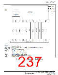
Section 13 Timer Z
Initial
Bit
Bit Name Value
R/W
Description
4
BFC0
0
R/W
Buffer Operation C0
0: GRC_0 operates normally
1: GRA_0 and GRC_0 are used together for buffer
operation
3 to 1
0
All 1
0
Reserved
These bits are always read as 1, and cannot be modified.
Timer Synchronization
SYNC
R/W
0: TCNT_1 and TCNT_0 operate as a different timer
counter
1: TCNT_1 and TCNT_0 are synchronized
TCNT_1 and TCNT_0 can be pre-set or cleared
synchronously
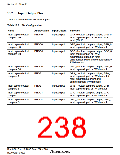
13.3.3
Timer PWM Mode Register (TPMR)
TPMR sets the pin to enter PWM mode.
Initial
Bit
Bit Name Value
R/W
Description
7
1
0
Reserved
This bit is always read as 1, and cannot be modified.
PWM Mode D1
6
5
4
3
PWMD1
R/W
R/W
R/W
0: FTIOD1 operates normally
1: FTIOD1 operates in PWM mode
PWM Mode C1
PWMC1
PWMB1
0
0
1
0: FTIOC1 operates normally
1: FTIOC1 operates in PWM mode
PWM Mode B1
0: FTIOB1 operates normally
1: FTIOB1 operates in PWM mode
Reserved
This bit is always read as 1, and cannot be modified.
Rev. 3.00 Sep. 10, 2007 Page 207 of 528
REJ09B0216-0300

 RENESAS [ RENESAS TECHNOLOGY CORP ]