Section 13 Timer Z
13.3.6
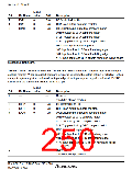
Timer Output Control Register (TOCR)
TOCR selects the initial outputs before the first occurrence of a compare match. Note that bits
OLS1 and OLS0 in TFCR set these initial outputs in reset synchronous PWM mode and
complementary PWM mode.
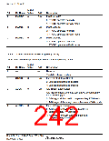
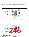
Initial
Bit
Bit Name Value
R/W
Description
7
TOD1
TOC1
TOB1
TOA1
TOD0
TOC0
TOB0
TOA0
0
0
0
0
0
0
0
0
R/W
Output Level Select D1
0: 0 output at the FTIOD1 pin*
1: 1 output at the FTIOD1 pin*
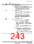
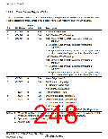
Output Level Select C1
6
R/W
R/W
R/W
R/W
R/W
R/W
R/W
0: 0 output at the FTIOC1 pin*
1: 1 output at the FTIOC1 pin*
Output Level Select B1
5
0: 0 output at the FTIOB1 pin*
1: 1 output at the FTIOB1 pin*
Output Level Select A1
4
0: 0 output at the FTIOA1 pin*
1: 1 output at the FTIOA1 pin*
Output Level Select D0
3
0: 0 output at the FTIOD0 pin*
1: 1 output at the FTIOD0 pin*
Output Level Select C0
2
0: 0 output at the FTIOC0 pin*
1: 1 output at the FTIOC0 pin*
Output Level Select B0
1
0: 0 output at the FTIOB0 pin*
1: 1 output at the FTIOB0 pin*
Output Level Select A0
0
0: 0 output at the FTIOA0 pin*
1: 1 output at the FTIOA0 pin*
Note:
*
The change of the setting is immediately reflected in the output value.
Rev. 3.00 Sep. 10, 2007 Page 212 of 528
REJ09B0216-0300

 RENESAS [ RENESAS TECHNOLOGY CORP ]