Section
Page
Description
10.2.13 MCS0 Control 258
Register (MCSCR0)
Description added
Bit 6—CS2/CS0 Select (CS2/0)
Only 0 should be used for the CS2/0 bit in MCSCR0. Either 0 or 1
may be used for MCSCR1 to MCSCR7.
10.3.4 Synchronous
DRAM Interface
290
310
Bank Active description added
… .In bank active mode, too, all banks become inactive after a
refresh cycle or after the bus is released as the result of bus
arbitration.
The bank active mode should not be used unless the bus width
for all areas is 32 bits.
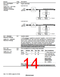
10.3.6 PCMCIA
Interface
Figure amended
D15 to D0
(Write)
Figure 10.32 Basic
Timing for PCMCIA
Memory Card Interface
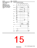
10.3.7 Waits between 320
Access Cycles
Figure amended
T1
T2
Twait
T1
T2
Twait
T1
T2
Figure 10.40 Waits
between Access Cycles
CKIO
A25 to A0
10.3.10 MCS[0] to
MCS[7] Pin Control
323
387
Description amended
This enables 32-, 64-, 128-, or 256-Mbit memory to be connected
to area 0 or area 2. However, only CS2/0 = 0 (area 0) should be
used for MCSCR0. Table 10.15 shows MCSCR0–MCSCR7
settings and MCS[0]–MCS[7] assertion conditions.
11.6 Usage Notes
Description added
13. DMAC transfers should not be performed in the sleep mode
under conditions other than when the clock ratio of Iφ (on-
chip clock) to Bφ (bus clock) is 1:1.
14. When the following three conditions are all met, the
frequency control register (FRQCR) should not be changed
while a DMAC transfer is in progress.
• Bits IFC2 to IFC0 are changed.
• STC2 to STC0 in FRQCR are not changed.
• The clock ratio of Iφ (on-chip clock) to Bφ (bus clock) after
the change is other than 1:1.
13.4.3 Precautions
when Using RTC
Module Standby
426
Newly added
Rev. 5.0, 09/03, page xii of xliv

 RENESAS [ RENESAS TECHNOLOGY CORP ]