Section
Page
Description
8.3.3 Precautions
when Using the Sleep
Mode
187
Newley added
8.5.1 Transition to
Module Standby
Function
191
210
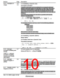
Note *3 added to bit table
Note: 3. Before putting the RTC into module standby status, first
access one or more of the RTC, SCI, and TMU
registers. The RTC may then be put into module standby
status.
9.3 Clock Operating
Modes
2. under cautions amended
The peripheral clock frequency should not be set higher than the
frequency of the CKIO pin, higher than 33.34 MHz.
Table 9.4 Available
Combinations of Clock
Mode and FRQCR
Values
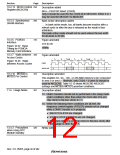
9.5.1 Changing the
Multiplication Rate
213
Description added
5.Supply of the clock that has been set begins at WDT count
overflow, and the processor begins operating again. The WDT
stops after it overflows.
When the following three conditions are all met, FRQCR should
not be changed while a DMAC transfer is in progress.
• Bits IFC2 to IFC0 are changed.
• STC2 to STC0 are not changed.
• The clock ratio of Iφ (on-chip clock) to Bφ (bus clock) after the
change is other than 1:1.
9.8.2 Changing the
Frequency
218,
219
Description added
5.The counter stops at a value of H'00 or H'01. The stop value
depends on the clock ratio.
When the following three conditions are all met, FRQCR should
not be changed while a DMAC transfer is in progress.
• Bits IFC2 to IFC0 are changed.
• STC2 to STC0 are not changed.
• The clock ratio of Iφ (on-chip clock) to Bφ (bus clock) after the
change is other than 1:1.
10.1.1 Features
223
246
Refresh function description deleted
Description added
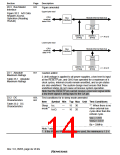
10.2.5 Individual
Memory Control
Register (MCR)
Bit 7—Synchronous DRAM Bank Active (RASD): Specifies
whether synchronous DRAM is used in bank active mode or auto-
precharge mode. Set auto-precharge mode when areas 2 and 3
are both designated as synchronous DRAM space.
The bank active mode should not be used unless the bus width
for all areas is 32 bits.
Rev. 5.0, 09/03, page xi of xliv

 RENESAS [ RENESAS TECHNOLOGY CORP ]