Section
Page
Description
20.3 Bus Master
Interface
622
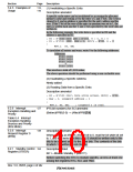
Figure amended
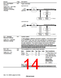
Upper byte read
Figure 20.2 A/D Data
Register Access
Operation (Reading
H'AA40)
CPU
receives
data H'AA
Module internal data bus
Bus
interface
TEMP
[H'40]
ADDRn H
[H'AA]
ADDRn L
n = A to D
[H'40]
Lower byte read
CPU
receives
data H'40
Module internal data bus
Bus
interface
TEMP
[H'40]
ADDRn H
[H'AA]
ADDRn L
n = A to D
[H'40]
23.1 Absolute
Maximum Ratings
657
Caution added
2.Until voltage is applied to all power supplies, a low level is input
at the RESETP pin, and CKIO has operated for a maximum of 4
clock cycles, internal circuits remain unsettled, and so pin states
are also undefined. The system design must ensure that these
undefined states do not cause erroneous system operation.
Note that the RESETP pin cannot receive a low level signal while
a low level signal is being input to the CA pin.
Table 23.1 Absolute
Maximum Ratings
23.2 DC
Characteristics
659,
662
Test conditions for in sleep mode amended
Item
Symbol Min Typ Max Unit Test Conditions
Table 23.2 DC
Characteristics
Sleep Icc
—
—
15 30
10 20
*1: When there is no
other external bus
cycle other than the
refresh cycle.
1
*
mode
IccQ
Vcc = 1.9 V
VccQ = 3.3 V
Bφ = 33MHz
Note * added
* If the IRL and IRLS interrupts are used, the minimum is 1.9 V.
Rev. 5.0, 09/03, page xiv of xliv

 RENESAS [ RENESAS TECHNOLOGY CORP ]