17.1.3 Pin Configuration
Table 17.1 shows the smart card interface pin configuration.
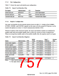
Table 17.1 Smart Card Interface Pins
Pin Name
Abbreviation
MD0/SCK
RxD
I/O
Function
Serial clock pin
Receive data pin
Transmit data pin
I/O
Clock input/output
Receive data input
Transmit data output
Input
Output
MD7/TxD
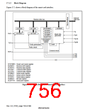
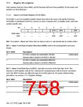
17.1.4 Register Configuration
The smart card interface has the internal registers shown in table 17.2. Details of the SCBRR1,
SCTDR1, SCRDR1, and SCSPTR1 registers are the same as for the normal SCI function: see the
register descriptions in section 15, Serial Communication Interface (SCI).
With the exception of the serial port register, the smart card interface registers are initialized in
standby mode and in the module standby state as well as by a power-on reset or manual reset.
When recovering from standby mode or the module standby state, the registers must be set again.
Table 17.2 Smart Card Interface Registers
Initial
Area 7
Access
Size
Name
Abbreviation R/W
Value P4 Address Address
Serial mode register
Bit rate register
Serial control register
SCSMR1
SCBRR1
SCSCR1
R/W
R/W
R/W
R/W
H'00
H'FF
H'00
H'FF
H'84
H'00
H'00
H'FFE00000 H'1FE00000
H'FFE00004 H'1FE00004
H'FFE00008 H'1FE00008
H'FFE0000C H'1FE0000C
H'FFE00010 H'1FE00010
H'FFE00014 H'1FE00014
H'FFE00018 H'1FE00018
8
8
8
8
8
8
8
Transmit data register SCTDR1
1
*
Serial status register
Receive data register
SCSSR1
SCRDR1
SCSCMR1
R/(W)
R
Smart card mode
register
R/W
2
*
Serial port register
SCSPTR1
R/W
H'00
H'FFE0001C H'1FE0001C
8
Notes: *1 Only 0 can be written, to clear flags.
*2 The value of bits 2 and 0 is undefined.
Rev. 6.0, 07/02, page 705 of 986

 RENESAS [ RENESAS TECHNOLOGY CORP ]