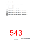
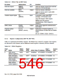
Table 14.2 DMAC Pins in DDT Mode
Pin Name
Abbreviation
I/O
Function
Data bus request
'%5(4
Input
Data bus release request from external
device for DTR format input
('5(43)
Data bus available
%$9/
Output
Input
Data bus release notification
(DRAK0)
Data bus can be used 2 cycles after
%$9/ is asserted
Transfer request signal 75
('5(44)
If asserted 2 cycles after %$9/
assertion, DTR format is sent
Only 75 asserted: DMA request
'%5(4 and 75 asserted
simultaneously: Direct request to
channel 2
DMAC strobe
7'$&.
Output
Output
Reply strobe signal for external device
from DMAC
(DACK0)
Channel number
notification
ID [1:0]
(DRAK1, DACK1)
Notification of channel number to
external device at same time as 7'$&.
output
(ID [1] = DRAK1, ID [0] = DACK1)
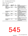
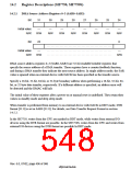
14.1.4 Register Configuration (SH7750, SH7750S)
Table 14.3 summarizes the DMAC registers. The DMAC has a total of 17 registers: four registers
are allocated to each channel, and an additional control register is shared by all four channels.
Table 14.3 DMAC Registers
Chan-
nel
Abbre-
viation
Read/
Write
2
Area 7
Access
Size
Name
Initial Value P4 Address Address
*
*
*
0
DMA source
address register 0
R/W
R/W
R/W
R/W
Undefined H'FFA00000 H'1FA00000 32
Undefined H'FFA00004 H'1FA00004 32
Undefined H'FFA00008 H'1FA00008 32
H'00000000 H'FFA0000C H'1FA0000C 32
SAR0
2
2
DMA destination
address register 0
DAR0
DMA transfer
count register 0
DMATCR0
CHCR0
*1 *2
DMA channel
control register 0
Rev. 6.0, 07/02, page 494 of 986

 RENESAS [ RENESAS TECHNOLOGY CORP ]