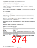
13.1.4 Register Configuration
The BSC has the 11 registers shown in table 13.2. In addition, the synchronous DRAM mode
register incorporated in synchronous DRAM can also be accessed as an SH7750 Series register.
The functions of these registers include control of interfaces to various types of memory, wait
states, and refreshing.
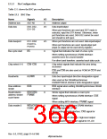
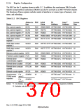
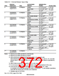
Table 13.2 BSC Registers
Abbrevia- R/W Initial
P4
Address
Area 7
Address
Access
Size
Name
tion
Value
Bus control register 1
Bus control register 2
Bus control register 3
Bus control register 4
BCR1
BCR2
BCR3
BCR4
WCR1
R/W H'0000 0000 H'FF80 0000 H'1F80 0000 32
R/W H'3FFC
R/W H'0000
H'FF80 0004 H'1F80 0004 16
H'FF80 0050 H'1F80 0050 16
2
2
*
*
R/W H'0000 0000 H'FE0A 00F0 H'1E0A 00F0 32
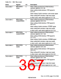
R/W H'7777 7777 H'FF80 0008 H'1F80 0008 32
Wait state control
register 1
Wait state control
register 2
WCR2
WCR3
R/W H'FFFE EFFF H'FF80 000C H'1F80 000C 32
R/W H'0777 7777 H'FF80 0010 H'1F80 0010 32
R/W H'0000 0000 H'FF80 0014 H'1F80 0014 32
Wait state control
register 3
Memory control register MCR
PCMCIA control register PCR
R/W H'0000
R/W H'0000
H'FF80 0018 H'1F80 0018 16
H'FF80 001C H'1F80 001C 16
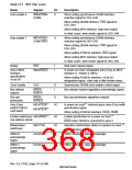
Refresh timer
RTCSR
control/status register
Refresh timer counter
RTCNT
RTCOR
R/W H'0000
R/W H'0000
H'FF80 0020 H'1F80 0020 16
H'FF80 0024 H'1F80 0024 16
Refresh time constant
counter
Refresh count register
RFCR
R/W H'0000
H'FF80 0028 H'1F80 0028 16
1
*
Synchronous For
SDMR2
W
—
H'FF90 xxxx H'1F90 xxxx
8
DRAM mode
registers
area 2
1
*
For
SDMR3
H'FF94 xxxx H'1F94 xxxx
area 3
Notes: *1 For details, see section 13.2.10, Synchronous DRAM Mode Registers (SDMR).
*2 Settable only for SH7750R.
Rev. 6.0, 07/02, page 318 of 986

 RENESAS [ RENESAS TECHNOLOGY CORP ]