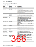
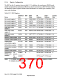
13.1.3 Pin Configuration
Table 13.1 shows the BSC pin configuration.
Table 13.1 BSC Pins
Name
Signals
I/O
O
Description
Address bus
Data bus
A25–A0
Address output
Data input/output
D63–D52,
D31–D0
I/O
When port functions are used and DDT mode is
selected, input the DTR format. Otherwise, when
port functions are used, D60-D52 cannot be used
and should be left open.
Data bus/port
Bus cycle start
D51–D32/
PORT19–
PORT0
I/O
O
When port functions are not used: data input/output
When port functions are used: input/output port
(input or output set for each bit by register)
%6
Signal that indicates the start of a bus cycle
When setting synchronous DRAM interface:
asserted once for a burst transfer
For other burst transfers: asserted each data cycle
Chip select 6–0
Read/write
&69–&63
O
O
Chip select signals that indicate the area being
accessed
&68 and &69 are also used as PCMCIA &(4$ and
&(4%
Data bus input/output direction designation signal
RD/:5
Also used as the DRAM/synchronous
DRAM/PCMCIA interface write designation signal
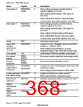
Row address
strobe
5$6
O
O
5$6 signal when setting DRAM/synchronous DRAM
interface
Read/column
address strobe/
cycle frame
5'/&$66/
Strobe signal that indicates a read cycle
)5$0(
When setting synchronous DRAM interface: &$6
signal
When setting MPX interface: )5$0( signal
Data enable 0
:(3/&$63/
O
When setting synchronous DRAM interface:
selection signal for D7–D0
DQM0
When setting DRAM interface: &$6 signal for
D7–D0
When setting MPX interface: high-level output
In other cases: write strobe signal for D7–D0
Rev. 6.0, 07/02, page 314 of 986

 RENESAS [ RENESAS TECHNOLOGY CORP ]