CENTRAL PROCESSING UNIT (CPU)
2.1 Central processing unit (CPU)
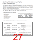
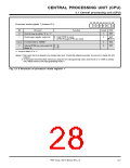
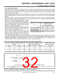
b7 b6 b5 b4 b3 b2 b1 b0
Processor mode register 1 (Address 5F16)
0 0 0 0
0
X
Bit
0
Bit name
Function
At reset
R/W
1
RW
This bit may be either “0” or “1.”
Direct page register switch bit
0 : Only DPR0 is used.
1 : DPR0 through DPR3 are used.
0
RW
(Note 1)
1
Fix these bits to “00000.”
0
0
RW
RW
6 to 2
7
0 : 3φ
1 : 2φ
Internal ROM bus cycle select bit
(Note 2)
X : It may be either “0” or “1.”
Notes 1: After reset, this bit is allowed to be changed only once. (During the software execution, be sure not to change this bit’s
content.)
2: To reprogram the internal flash memory by using the CPU reprogramming mode, clear this bit to “0.” (Refer to section
“19.2 Flash memory CPU reprogramming mode.”)
Fig. 2.1.5 Structure of processor mode register 1
7906 Group User’s Manual Rev.2.0
2-7

 RENESAS [ RENESAS TECHNOLOGY CORP ]