CENTRAL PROCESSING UNIT (CPU)
2.1 Central processing unit (CPU)
2.1.5 Program counter (PC)
The program counter is a 16-bit counter that indicates the low-order 16 bits of the address (24 bits) at
which an instruction to be executed next (in other words, an instruction to be read out from an instruction
queue buffer next) is stored. The contents of the high-order program counter (PC
H
) become “FF16,” and the
low-order program counter (PC ) becomes “FE16” at reset. The contents of the program counter becomes
L
the contents of the reset’s vector address (addresses FFFE16, FFFF16) just after reset.
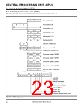
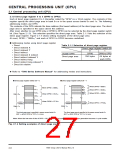
Figure 2.1.3 shows the program counter and the program bank register.
(b23)
b7
(b16)
b0 b15
b8 b7
b0
PG
PCH
PCL
Fig. 2.1.3 Program counter and Program bank register
2.1.6 Program bank register (PG)
The memory space is divided into units of 64 Kbytes. This unit is called “bank.” (Refer to section “2.3
Access space.”)
The program bank register is an 8-bit register that indicates the high-order 8 bits of the address (24 bits)
at which an instruction to be executed next (in other words, an instruction to be read out from an instruction
queue buffer next) is stored. These 8 bits indicate a bank.
When a carry occurs after adding the contents of the program counter or adding the offset value to the
contents of the program counter in the branch instruction and others, the contents of the program bank
register is automatically incremented by 1. When a borrow occurs after subtracting the contents of the
program counter, the contents of the program bank register is automatically decremented by 1. Therefore,
there is no need to consider bank boundaries during programming, usually.
This register is cleared to “0016” at reset.
2.1.7 Data bank register (DT)
The data bank register is an 8-bit register. In the following addressing modes using the data bank register,
the contents of this register is used as the high-order 8 bits (bank) of a 24-bit address to be accessed.
Use the LDT instruction when setting a value to this register.
This register is cleared to “0016” at reset.
❈ Addressing modes using data bank register
•Direct indirect
•Direct indexed X indirect
•Direct indirect indexed Y
•Absolute
•Absolute indexed X
•Absolute indexed Y
•Absolute bit relative
•Stack pointer relative indirect indexed Y
•Multiplied accumulation
❈ Refer to “7900 Series Software Manual” for addressing modes.
7906 Group User’s Manual Rev.2.0
2-5

 RENESAS [ RENESAS TECHNOLOGY CORP ]