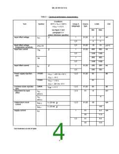
MIL-M-38510/131A
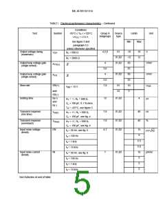
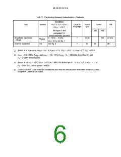
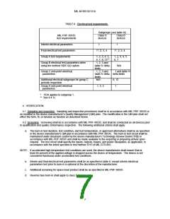
TABLE I. Electrical performance characteristics.
Conditions
-55°C ≤ T ≤ +125°C
Test
Symbol
Group A
subgroups
Device
type
Limits
Unit
A
±V
CC
= ±15 V,
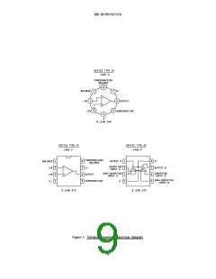
see figure 3 and
paragraph 3.5
Min
Max
unless otherwise specified
1/
Input offset voltage
1
2,3
2,3
1
01,02
-2
-3
2
mV
V
IO
3
Input offset voltage
temperature sensitivity
Input bias current
01,02
01,02
-10
10
µV/°C
∆V /∆t
IO
1/
1/
-800
-1500
-800
-1500
-200
-500
85
800
1500
800
1500
200
500
nA
+I
IB
2,3
1
-I
IB
2,3
1
Input offset current
01,02
01,02
nA
dB
I
IO
2,3
1,2,3
Power supply rejection
ratio
+PSRR
-PSRR
CMRR
+V
= +20 V to +10 V,
= -15 V
CC
-V
CC
85
+V
= +15 V,
CC
-V
CC
= -20 V to -10 V
Common mode rejection
ratio
Adjustment for input
offset
1,2,3
1,2,3
01,02
01
80
+4
dB
V
CM
= ±11 V
mV
V
IO
(ADJ+)
-4
V
IO
(ADJ-)
Output short circuit
current
1,2,3
1
01,02
-95
mA
mA
t ≤ 25 ms 4/
t ≤ 25 ms 4/
I
I
I
OS(+)
OS(-)
CC
+95
6.5
Supply current
01
02
01
02
11.0
9.0
2,3
13.0
See footnotes at end of table.
4

 RAYTHEON [ RAYTHEON COMPANY ]