VRS51C1000
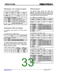
PWM Registers - Port1 Configuration Register
PWM Data Registers
TABLE 39: PORT1 CONFIGURATION REGISTER (PWME, $9B)
The following tables describe the PWM Data
Registers. The PWMDx bits hold the content of the
PWM Data Register and determine the duty cycle of
the PWM output waveforms. The NP[2:0] bits will insert
narrow pulses into the 8-PWM-cycle frame.
7
6
5
4
PWM4E
PWM3E
PWM2E
PWM1E
3
2
1
0
PWM0E
Unused
TABLE 41: PWM DATA REGISTER 0 (PWMD0) – SFR A4H
Bit
Mnemonic
PWM4E
PWM3E
PWM2E
PWM1E
PWM0E
Description
When bit is set to one, the
7
6
5
4
7
6
5
4
3
PWMD0.4
PWMD0.3
PWMD0.2
PWMD0.1
corresponding PWM pin is active as
a PWM function. When the bit is
cleared, the corresponding PWM pin
is active as an I/O pin. These five
bits are cleared upon reset.
-
3
2
1
0
PWMD0.0
NP0.2
NP0.1
NP0.0
Bit Mnemonic
Description
[2:0]
Unused
7
6
5
4
3
2
1
0
PWMD0.4
PWMD0.3
PWMD0.2
PWMD0.1
PWMD0.0
NP0.2
Contents of PWM Data Register 0 Bit 4
Contents of PWM Data Register 0 Bit 3
Contents of PWM Data Register 0 Bit 2
Contents of PWM Data Register 0 Bit 1
Contents of PWM Data Register 0 Bit 0
Inserts Narrow Pulses in a 8-PWM-Cycle
Frame
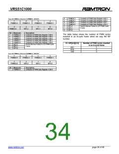
PWM Registers -PWM Control Register
The following table describes the PWM Control
Register.
NP0.1
NP0.0
TABLE 42: PWM DATA REGISTER 1 (PWMD1) – SFR A5H
TABLE 40: PWM CONTROL REGISTER (PWMC) – SFR A3H
7
6
5
4
7
6
5
4
3
2
1
0
PWMD1.4
PWMD1.3
PWMD1.2
PWMD1.1
PDCK1
PDCK0
Unused
3
2
1
0
Bit
[7:2]
1
Mnemonic
Unused
PDCK1
Description
-
Input Clock Frequency Divider Bit 1
Input Clock Frequency Divider Bit 0
PWMD1.0
NP1.2
NP1.1
NP1.0
Bit Mnemonic
Description
0
PDCK0
7
6
5
4
3
2
1
0
PWMD1.4
PWMD1.3
PWMD1.2
PWMD1.1
PWMD1.0
NP1.2
Contents of PWM Data Register 1 Bit 4
Contents of PWM Data Register 1 Bit 3
Contents of PWM Data Register 1 Bit 2
Contents of PWM Data Register 1 Bit 1
Contents of PWM Data Register 1 Bit 0
Inserts Narrow Pulses in a 8-PWM-Cycle
Frame
The following table describes the relationship between
the values of PDCK1/PDCK0 and the value of the
divider. Numerical values of the corresponding
frequencies are also provided.
NP1.1
NP1.0
PDCK1 PDCKO
Divider
PWM clock,
Fosc=20MHz
10MHz
5MHz
2.5MHz
1.25MHz
PWM clock,
Fosc=24MHz
12MHz
TABLE 43: PWM DATA REGISTER 2 (PWMD2) – SFR A6H
0
0
1
1
0
1
0
1
2
4
8
7
6
5
4
6MHz
3MHz
1.5MHz
PWMD2.4
PWMD2.3
PWMD2.2
PWMD2.1
16
3
2
1
0
PWMD2.0
NP2.2
NP2.1
NP2.0
Bit Mnemonic
Description
7
6
5
4
3
2
1
0
PWMD2.4
PWMD2.3
PWMD2.2
PWMD2.1
PWMD2.0
NP2.2
Contents of PWM Data Register 2 Bit 4
Contents of PWM Data Register 2 Bit 3
Contents of PWM Data Register 2 Bit 2
Contents of PWM Data Register 2 Bit 1
Contents of PWM Data Register 2 Bit 0
Inserts Narrow Pulses in a 8-PWM-Cycle
Frame
NP2.1
NP2.0
______________________________________________________________________________________________
www.ramtron.com page 33 of 48

 RAMTRON [ RAMTRON INTERNATIONAL CORPORATION ]