64Mbit – Enhanced SDRAM
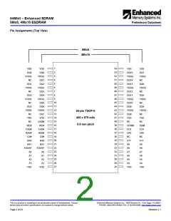
8Mx8, 4Mx16 ESDRAM
Preliminary Datasheet
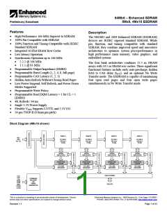
General Description
The 64Mbit ESDRAM is a high-speed SDRAM configured as four banks of DRAM with an SRAM row cache per bank
and a synchronous interface. All inputs are registered and all outputs are driven on the rising edge of clock. Within each
bank, the devices are organized as 4096 rows of 4096 bits each. Within each row, the 8Mx8 device has 512 column
address locations and the 4Mx16 device has 256 column locations.
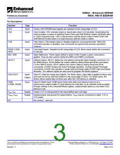
Read and write accesses are accomplished by opening a row and selecting a column address location for the transaction.
The Bank Activate command instructs the device to open a row in one of the four banks, though all four banks may be
active simultaneously. A subsequent Read or Write command instructs the device to read data from or write data to a
specified column address location.
The device can be programmed to burst data in or out. Burst accesses start with the given column address location and
continue until the burst length is satisfied. Throughout the burst, the device internally generates column addresses
according to the burst type and burst length programmed into the Mode register.
An early auto-precharge feature allows the device to self-time its row precharge one clock cycle after a Read command is
issued, and one clock cycle following the last data word in a write burst. A precharge operation must occur before another
row is opened within the same bank.
Row Cache Operation
The ESDRAM architecture combines four banks of fast 22.5 ns DRAM with a 10.5 ns SRAM row cache per bank to
improve memory latency. Sustained high-speed bandwidth is achieved by pipelining operations internally. On a random
read access, a DRAM bank is activated and data is latched into the sense amplifiers in 12 ns. The sense amplifiers now
hold a row of data and the row is considered open. A Read command now causes the entire row to latch into the SRAM
row cache, and the data at the specified column address location is driven out in 10.5 ns.
Since the row data is latched into the SRAM row cache, the DRAM sense amplifiers are decoupled from the data. So the
DRAM precharge time can be hidden behind a burst read from the row cache. This minimizes subsequent page miss
latency. Since both precharge and RAS to CAS delays are hidden, the device supports an industry leading CAS latency of
one at clock frequencies up to 83 MHz, and CAS latency of two up to 166 MHz.
At 166 MHz, all but one cycle of the next random access to any location in the same bank can be hidden. This
dramatically increases sustained bandwidth by up to two times over standard SDRAM. For interleaved burst read
accesses, the entire precharge time is hidden and output data can be driven without any wait states.
No Write Transfer Mode
The ESDRAM architecture offers the system designer two different cache loading policies during write cycles. The cache
loading policy is programmed via the Mode Register Set command.
In Write Transfer (normal) mode the SRAM row cache is always loaded with the write data. This ensures coherency
between the row cache and the DRAM array, and allows read-modify-write cycles and simplified memory control logic.
In No Write Transfer mode, the row cache is not loaded during writes to the DRAM array. This allows continued access
to the previously cached read data without incurring a page miss penalty (closing the write row and re-opening the read
row). The ESDRAM can maintain four open read pages and four open write pages simultaneously in No Write Transfer
mode. This subject is also covered in the section on the Mode Register Set command.
Note: If a write hit occurs (the write page is already in the cache) the ESDRAM automatically updates the cache when the
data is written to the DRAM array, regardless of the Write Transfer mode setting. This maintains coherency.
This is a product in sampling or pre-production phase of development. Charac-
teristic data and other specifications are subject to change without notice.
Enhanced Memory Systems Inc., 1850 Ramtron Dr., Colo Spgs, CO 80921
PHONE: (800) 545-DRAM; FAX: (719) 488-9095; http://www.edram.com
Page 4 of 33
Revision 1.1

 RAMTRON [ RAMTRON INTERNATIONAL CORPORATION ]