64Mbit – Enhanced SDRAM
8Mx8, 4Mx16 ESDRAM
Preliminary Datasheet
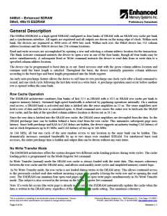
Mode Register Set (Address Input for Mode Set)
BA1
BA0
A11
A10
A9
A8
A7
A6
A5
A4
A3
BT
A2
A1
A0
Write Policy
CAS Latency
Burst Length
BA1
0
BA0
0
M11
0
M10
0
M9
0
M8
0
M7
0
Mode
M3
0
Burst type
Write
Sequential
Interleaved
Transfer
No Write
0
0
0
0
1
0
0
1
Transfer
Burst Length
M2
M1
M0
M6
0
M5
0
M4
0
CAS Latency
Reserved
1
Sequential
Interleaved
0
0
0
0
1
1
1
1
0
0
1
1
0
0
1
1
0
1
0
1
0
1
0
1
1
1
0
0
1
2
2
0
1
0
2
4
4
0
1
1
3
8
8
1
0
0
Reserved
Reserved
Reserved
Reserved
Reserved
Reserved
Reserved
Full Page
Reserved
Reserved
Reserved
Reserved
1
0
1
1
1
0
1
1
1
CAS Latency
The CAS latency refers to the delay from when a Read command is registered on a rising clock edge to when the data
becomes available at the outputs. CAS latency is expressed in clock cycles, and can have values of one, two, or three
cycles. A table showing these relationships appears in the Electrical Characteristics section.
Write Policy
There are two modes that define how the ESDRAM row cache is used during write cycles. In Write Transfer mode, the
row cache is always loaded with the write data during write cycles. This assures coherency between the row cache and the
DRAM array, allowing read-modify-write cycles and simplified memory control logic.
In No Write Transfer mode, the row cache is not loaded with the write data during a Write command execution. Data is
written to the DRAM array, but the prior row cache contents are maintained. Every time the memory controller issues a
Bank Activate command, the ESDRAM loads an internal row address register for later comparison against a new row
address during the next Bank Activate command. If the on-chip page hit/miss comparator determines that the write is to
the same row as the one in the row cache, the write updates the row cache along with the DRAM array to maintain
coherency.
No Write Transfer mode allows immediate return to the prior cached read page without incurring a page miss penalty. If a
cache read follows a write cycle, write precharge time can be hidden.
This is a product in sampling or pre-production phase of development. Charac-
teristic data and other specifications are subject to change without notice.
Enhanced Memory Systems Inc., 1850 Ramtron Dr., Colo Spgs, CO 80921
PHONE: (800) 545-DRAM; FAX: (719) 488-9095; http://www.edram.com
Page 8 of 33
Revision 1.1

 RAMTRON [ RAMTRON INTERNATIONAL CORPORATION ]