64Mbit – Enhanced SDRAM
8Mx8, 4Mx16 ESDRAM
Preliminary Datasheet
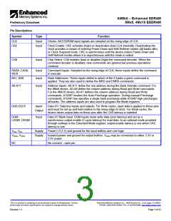
Pin Descriptions
Symbol
CLK
CKE
Type
Function
Input
Input
Clocks: All ESDRAM input signals are sampled on the rising edge of CLK.
Clock Enable: CKE activates (high) or deactivates (low) CLK internally. Deactivating the
clock provides a means of entering Power-Down and Self-Refresh modes (all banks idle),
or Clock Suspend mode. CKE is synchronous until the device enters Power-Down and
Self-Refresh modes where it is asynchronous until the mode is exited.
CS#
Input
Chip Select: CS# enables (low) or disables (high) the command decoder. When the
command decoder is disabled, new commands are ignored but previous operations
continue.
RAS#, CAS#,
WE#
BA1, BA0
Input
Input
Input
Command Inputs: Sampled on the rising edge of CLK, these inputs define the command
to execute.
Bank Addresses: These inputs define to which of the 4 banks a given command is
applied. They are also used to define the MRS and EMRS commands.
A0-A11
Address Inputs: A0-A11 define the row address during the Bank Activate command. For
the 8Mx8 device, A0-A8 define the column address during Read and Write commands.
For the 4Mx16 device, A0-A7 defines the column address during Read and Write
commands. A10/AP invokes the Auto-Precharge operation. During manual Precharge
commands, A10/AP low specifies a single bank precharge while A10/AP high precharges
all banks. The address inputs are also used to program the Mode registers.
DQ0-DQ15
Input/
Output
Data I/O: Data bus inputs and outputs. For Write cycles, input data is applied to these pins
and must be set up and held relative to the rising edge of clock. For Read cycles, the
device drives output data on these pins after the CAS latency is satisfied.
DQM
Input
Data I/O Mask Input: DQM inputs mask write data (zero latency) and act as a
synchronous output enable (2-cycle latency) for read data. In an optional mode provided
through settings in the Extended Mode register, output enable latency is one when CAS
latency is one.
LDQM, UDQM
VDD, VSS
VDDQ, VSSQ
Supply
Supply
Power (+3.3 V) and ground for the input buffers and core logic.
Isolated power and ground for output buffers. VDDQ may be connected to either 3.3V or
2.5V power.
NC
-
No connect - open pin.
This is a product in sampling or pre-production phase of development. Charac-
teristic data and other specifications are subject to change without notice.
Enhanced Memory Systems Inc., 1850 Ramtron Dr., Colo Spgs, CO 80921
PHONE: (800) 545-DRAM; FAX: (719) 488-9095; http://www.edram.com
Revision 1.1
Page 3 of 33

 RAMTRON [ RAMTRON INTERNATIONAL CORPORATION ]