16Mbit ESDRAM Family
can begin auto-precharge of the current DRAM bank at
cycle T3, one cycle after the read command. This is the
direct result of having a row cache. The read command
automatically loads the row cache allowing the data burst
to come from the cache while the DRAM is free to
prepare the next random access. The ESDRAM has
completed its precharge by T5, so the ESDRAM is ready
for the next random access at that time. The next read
access can occur concurrently with the last few words of
the first burst. The second burst read begins at T9,
eleven cycles earlier than SDRAM. The ESDRAM can
move 2.6 times more random data over the data bus at
133MHz due to its faster memory speed and its ability to
efficiently pipeline random access cycles.
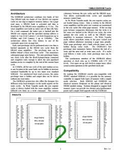
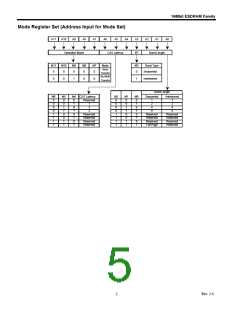
ESDRAM Concurrent Operations
Improve System Performance
The ESDRAM’s row cache allows unique concurrent
operations not supported by the industry standard
SDRAM. The timing diagram below describes the ability
of the ESDRAM to fully pipeline random row read bursts
to the same bank at 133MHz.
The top timing diagram shows the SDRAM
performing a bank activate at T0. The SDRAM must
wait until T3 for a read command (RCD Latency = 3).
The first word of the four-word burst reaches the output
pins 3 cycles after the read command (CAS Latency = 4).
The SDRAM cannot begin to precharge the current
DRAM bank until one cycle before the end of the current
burst. Following the auto-precharge cycle, the next data
burst from the same bank cannot start until T20. The
SDRAM incurs a total of 9 dead bus cycles on back to
back random reads at 133MHz.
In addition to pipelining random access read cycles,
ESDRAM also improves system performance by
allowing:
· Hidden Refresh Cycles During Cache Reads
· Hidden Precharge and Bank Activate for a Write Miss
Following Cache Reads
· Reduced Precharge and Bank Activate Latency on
Back to Back Write Miss Cycles
The ESDRAM also activates its bank at T0. Because
of the faster ESDRAM array, the read command can start
at T2 (RCD Latency = 2). The first word of the four-
word burst reaches the output pins 2 cycles after the read
command (CAS Latency = 2). ESDRAM initial latency
is 75% faster than SDRAM at 133MHz. The ESDRAM
· Immediate Access to Cache Reads while DRAM Page
is Closed
Random Row Read to the Same Bank at 133MHz, BL=4
CLK
SDRAM Command
DQ
ACT
ACT
R-AP
ACT
R-AP
1
2
3
4
1
2
3
3
4
ESDRAM Command
DQ
R-AP
ACT
2
R-AP
4
ACT
2
R-AP
4
ACT
2
R-AP
4
ACT
2
R-AP
4
1
3
1
3
1
3
1
1
Rev. 2.4
8

 RAMTRON [ RAMTRON INTERNATIONAL CORPORATION ]