16Mbit ESDRAM Family
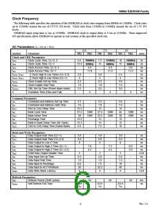
Clock Frequency
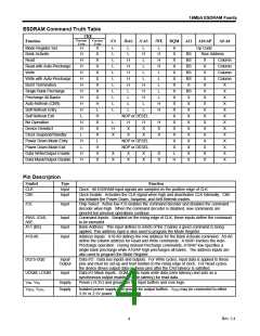
The following table specifies the operation of the ESDRAM at clock rates ranging from 66MHz to 150MHz. Clock rates
up to 133MHz assume the use of LVTTL I/O levels. Clock rates from 133MHz to 150MHz assume the use of 2.5V I/O
levels.
ESDRAM input setup time is 2ns at 133MHz. ESDRAM clock to output delay is 4.5ns at 133MHz. These improved
I/O specifications allow ESDRAM to operate in real systems at the specified clock rate.
AC Parameters (TA = 0°C to + 70°C)
-6.6
-7.5
-10
Symbol
Parameter
Min
Max
Min
Max
Min
Max
Units
Clock and CKE Parameters
tCK2
Clock Cycle Time, CL=2, 3
6.6
13.3
-
7.5
15
-
10
15
-
ns
ns
ns
ns
ns
ns
ns
ns
ns
ns
150MHz
133MHz
100MHz
tCK1
Clock Cycle Time, CL=1
83MHz
66MHz
66MHz
tAC2
Clock Access Time, CL=2, 3
Clock Access Time, CL=1
4.3
4.5
5.0
tAC1
-
11.0
-
11.5
-
11.5
tCKH2, tCKL2
tCKH1, tCKL1
tCKES
tCKEH
tCKESP
tT
Clock High & Low Times (CL=2,3)
Clock High & Low Times (CL=1)
Clock Enable Set-Up Time
2.8
4
-
-
2.8
5
-
-
3.5
5
-
-
2.2
1.0
2.2
-
-
2.2
1.0
2.2
-
-
3.0
1.0
3.0
-
-
Clock Enable Hold Time
-
-
-
CKE Set-Up Time (Power down mode)
Transition Time (Rise and Fall)
-
-
-
4
4
4
Common Parameters
tCS
Command and Address Set-Up Time
2.2
1.0
-
2.2
1.0
15
-
3.0
1.0
15
45
30
15
15
10
-
ns
ns
ns
ns
ns
ns
ns
ns
tCH
Command and Address Hold Time
RAS to CAS Delay Time
Bank Cycle Time
-
-
-
tRCD
tRC
tRAS
tRP
tRRD
tCCD
13.3
37.5
20
-
-
-
120K
37.5
22.5
15
120K
120K
Bank Active Time
120K
120K
120K
Precharge Time
13.3
13.3
6.6
-
-
-
-
-
-
-
-
-
Bank to Bank Delay Time (Alt. Bank)
CAS to CAS Delay Time (Same Bank)
15
7.5
Read and Write Parameters
tOH1
tOH2
tLZ
Data Output Hold Time (CL=1)
3.0
2.0
0
-
3.0
2.0
0
-
3.0
2.0
0
-
ns
ns
Data Output Hold Time (CL=2,3)
Data Output to Low-Z Time
Data Output to High-Z Time (CL=1)
Data Output to High-Z Time (CL=2,3)
DQM Data Output Disable Time
Data Input Set-Up Time
-
-
-
-
-
-
ns
tHZ1
tHZ2
tDQZ
tDS
-
7.0
-
7.5
-
8.0
ns
-
4.3
-
4.5
-
5.0
ns
2
-
-
-
-
-
-
2
-
-
-
-
-
-
2
-
-
-
-
-
-
CLK
ns
2.0
1.0
6.6
20
0
2.0
1.0
7.5
22.5
0
2.0
1.0
10
30
0
tDH
Data Input Hold Time
ns
tDPL
tDAL
tDQW
Data Input to Precharge
ns
Data Input to ACTV/Refresh
Data Write Mask Latency
ns
CLK
Refresh Parameters
tREF
Refresh Period (2048 cycles)
-
64
-
-
64
-
-
64
-
ms
ns
2CLK
+tRC
2CLK
+tRC
2CLK
+tRC
tSREX
Self Refresh Exit Time
Rev. 2.4
6

 RAMTRON [ RAMTRON INTERNATIONAL CORPORATION ]