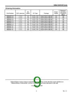
16Mbit ESDRAM Family
Single Bank Precharge - The ESDRAM will perform
a manual precharge of the bank specified by A11 (BS)
while A10/AP is low. Manual precharge terminates a
burst read after a delay equal to the CAS latency. It will
also terminate a burst write and mask data in the current
cycle.
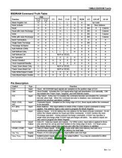
Basic Operating Modes
The ESDRAM operating modes are specified in the
following text and in the table below.
Hit and Miss Terminology - “Hit” and “miss” refer to
whether or not a new row address presented to the
ESDRAM matches a row already activated in the device.
There are up to two rows or “pages” that can be open at
any given point in time. The row data or page contents
consist of 4096 bits and are held in each bank’s sense
amplifiers. Each page is selected by the bank select pin
A11 (BS). Each bank’s SRAM row cache is loaded only
when a read command is issued. The ESDRAM’s on-chip
row address comparator is used only in No Write Transfer
mode of operation.
Precharge All Banks - The ESDRAM will precharge
both open banks if A10/AP is high. It will terminate burst
cycles exactly the same as the Single Bank Precharge
command.
Auto Refresh (CBR) - The ESDRAM will perform an
internal refresh cycle on both DRAM banks. Both banks
must be closed before this command is executed. Unlike
standard SDRAM, this command can be executed while
performing cache burst reads. The contents of each row
cache are not lost during Auto Refresh cycles.
The memory controller typically stores page (row)
address tags in order to determine which command to
issue based on the tag compare result.
Self Refresh Entry
-
The ESDRAM enters a self
Mode Register Set - Two mode registers are loaded
from pins A11 (BS) and A10-A0 when /CS, /RAS, /CAS,
and /WE are low. The standard mode register specifies
the burst length, burst type, CAS latency, and write
transfer mode.
refresh mode with refresh cycles automatically generated
by an internal clock. Self Refresh mode continues as long
as CKE is low. All input buffers except CKE are disabled.
The chip is in a low power standby mode.
Device Deselect - When /CS is high, the command
decoder is disabled but the prior command will be
completed (i.e. a burst will complete).
Bank Activate - A11 (BS) specifies one of the two
banks and the row address A10-A0 specifies which of the
2048 rows to load into its sense amplifiers. In No Write
Transfer mode, the ESDRAM compares the last row read
address to the current row address. If the two row
addresses match, a subsequent write updates the SRAM
row cache in addition to the DRAM. If the row addresses
do not match, only the DRAM is written.
Clock Suspend/Standby Mode - When CKE is low,
the internal execution of the current command is
suspended until CKE returns high.
Power Down Entry/Exit - If both DRAM banks are
precharged, CKE is low, and /CS is high, the chip will
enter its power down mode. Once the chip is in power
down mode, the chip will exit power down mode one clock
after CKE is returned high.
Write - The ESDRAM performs a write or burst write to
the bank specified by A11 (BS) and begins writing at the
start address specified by the column address A9-A0. If
the A10/AP pin is high, the auto-precharge operation
begins one cycle following the last write of the burst.
Note: In No Write Transfer mode, if the on-chip hit/miss
comparator result (from ACTV cycle) indicates a page hit,
then the write is performed to both the row cache and the
DRAM.
Data Write/Output Enable
-
When DQM is low,
write data is written to the chip during a write command
and the output buffers are enabled during read commands.
DQM latency is two cycles for reads and zero cycles for
writes.
Read - The ESDRAM loads the row cache and performs
a read or burst read from the cache to the bank specified
by A11 (BS) and begins reading at the start address
specified by the column address A9-A0. If the A10/AP
pin is high, the auto-precharge operation begins one cycle
following this command. The first read data is output
from the memory after the CAS latency (defined by the
Mode Register Set) has been satisfied.
Data Mask/Output Disable - When DQM is high,
write data is masked during a write command and the
output buffers are disabled during read commands. DQM
latency is two cycles for reads and zero cycles for writes.
Burst Terminate - The ESDRAM terminates a burst
read after a delay equal to the CAS latency. It will
terminate a burst write and mask data in the current cycle.
Rev. 2.4
3

 RAMTRON [ RAMTRON INTERNATIONAL CORPORATION ]