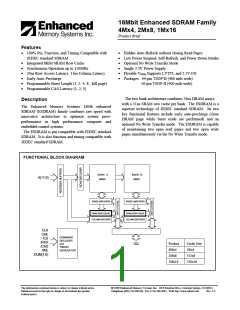
16Mbit ESDRAM Family
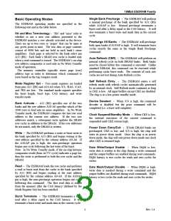
ESDRAM Command Truth Table
CKE
Previous
Cycle
Current
Cycle
Function
/CS
/RAS
/CAS
/WE
DQM
A11
A10/AP
A9-A0
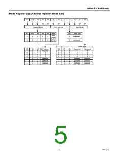
Mode Register Set
Bank Activate
H
H
H
H
H
H
H
H
H
H
H
L
X
X
X
X
X
X
X
X
X
H
L
L
L
L
L
L
L
L
L
L
L
L
L
L
L
H
L
L
H
H
H
L
X
X
X
X
X
X
X
X
X
X
X
X
X
X
X
X
X
L
Op Code
BS
BS
BS
BS
BS
X
Row Address
Read
H
H
H
H
H
L
X
X
X
X
X
X
X
X
X
X
X
X
X
X
X
X
X
Column
Read with Auto-Precharge
Write
L
Column
L
Column
Write with Auto-Precharge
Burst Termination
Single Bank Precharge
Precharge All Banks
Auto-Refresh (CBR)
Self Refresh Entry
Self Refresh Exit
L
L
Column
H
H
H
L
L
X
X
X
X
X
X
X
X
X
X
X
X
X
L
BS
X
L
L
L
H
H
X
L
L
X
H
X
X
X
L
NOP or DESEL
X
No Operation
H
H
L
L
H
X
H
X
X
H
X
X
H
X
X
X
Device Deselect
X
Clock Suspend/Standby
Power Down Mode Entry
Power Down Mode Exit
Data Write/Output Enable
Data Mask/Output Disable
X
H
L
NOP or DESEL
NOP or DESEL
X
H
X
X
X
H
H
X
X
X
X
X
X
X
X
X
H
X
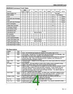
Pin Description
Symbol
Type
Input
Input
Function
CLK
Clock: All ESDRAM input signals are sampled on the positive edge of CLK.
CKE
Clock Enable: Activates the CLK signal when high and deactivates CLK internally. CKE
low initiates the Power Down, Suspend, and Self-Refresh modes.
/CS
Input
Chip Select: Active low /CS enables the command decoder and disables the command
decoder when high. When the command decoder is disabled, new commands are
ignored but previous operations continue.
/RAS, /CAS,
/WE
A11 (BS)
Input
Input
Input
Command Inputs: Sampled on the rising edge of CLK, these inputs define the command
to be executed.
Bank Address: This input defines to which of the 2 banks a given command is being
applied. This address input is also used to program the Mode Register.
Address Inputs: A10-A0 defines the row address for the Bank Activate command. A9-A0
define the column address for Read and Write commands. A10/AP invokes the Auto-
Precharge operation. During manual Precharge commands, A10/AP low specifies a
single bank precharge while A10/AP high precharges all banks. The address inputs are
also used to program the Mode Register.
A10-A0
DQ15-DQ0
Input/
Output
Data I/O: Data bus inputs and outputs. For Write cycles, input data is applied to these
pins and must be set-up and held relative to the rising edge of clock. For Read cycles,
the device drives output data on these pins after the CAS latency is satisfied.
Data I/O Mask Inputs: DQM inputs mask write data (zero latency) and acts as a
synchronous output enable (2 cycle latency) for read data.
UDQM, LDQM
Input
VDD, VSS
Supply
Supply
Power (+3.3V) and ground for the input buffers and core logic.
VDDQ, VSSQ
Isolated power supply and ground for output buffers. VDDQ may be connected to either
3.3V or 2.5V power.
Rev. 2.4
4

 RAMTRON [ RAMTRON INTERNATIONAL CORPORATION ]