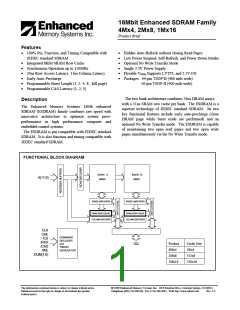
16Mbit ESDRAM Family
coherency between the row cache and the DRAM array.
This allows read-modify-write cycles and simplified
memory control logic.
Architecture
The ESDRAM architecture combines two banks of fast
24ns DRAM with two banks of 11ns SRAM row register
cache on one chip to improve memory latency. On a page
read miss, a DRAM bank is activated and data is
developed by the DRAM sense amplifiers in 13.3ns. The
sense amplifiers now hold an entire row of data (4K bits).
On a read command, the entire row is latched into the
SRAM row register and the specified starting address is
output in 11ns (CAS Latency 1 at clock frequencies up to
83MHz, and CAS Latency 2 up to 150MHz). The
architecture allows fast 11ns latency to any of the
constantly open rows on page hits.
In No Write Transfer mode, the row register caches are
not loaded during writes. Data is written to the DRAM
sense amplifiers and the prior row contents are maintained
in the row cache (for write page misses). If the on-chip
page hit/miss comparator determines that the write is to
the same row latched in the SRAM row cache, the write
updates the row cache as well as the DRAM sense
amplifiers to maintain coherency. No Write Transfer
mode allows immediate return to the prior cached read
page without otherwise incurring a page miss penalty.
Write page precharge and a bank activate times can be
Early auto-precharge can be performed since row data is
latched separately in the SRAM row cache from the
DRAM sense amplifiers. The precharge time can be
hidden behind a burst read from cache. This minimizes
subsequent page miss latency. The auto-precharge begins
one clock cycle after the Read-Autoprecharge command
and completes early enough to allow the next pipelined
random access to complete by the end of the current burst
cycle.
At 150MHz, all but one cycle of the next random access
to any location in the same bank can be hidden to increase
sustained bandwidth by up to two times over standard
SDRAM. For interleaved burst read accesses, the entire
precharge time is hidden and output data can be driven
without any wait states.
hidden during cache reads.
The ESDRAM’s fast
precharge time minimizes latency between the end of a
write and the next read or write miss cycle. If a cache
read follows a write cycle, write precharge time can be
hidden.
The synchronous interface of the ESDRAM allows
operation at clock rates up to 150MHz with 2.5V I/O
levels. Fast input set-up and clock-to-output times allow
actual system operation at the specified clock rate.
Compatibility
By making the ESDRAM exactly pin-compatible with
JEDEC standard SDRAM, it is possible for the memory
controller to support both types of memory with a simple
The ESDRAM architecture also offers the designer two
different cache load strategies via the mode register set for
write cycles. In Write Transfer mode, the row register
cache is always loaded with the sense amplifier contents
(DRAM row data) on a write command. This ensures
mode selection.
Both SDRAM and ESDRAM use
identical memory footprints on the planar and identical
DIMM module wiring. Systems designed to support both
memory types can provide two distinct price/performance
points and a simple field upgrade with the ESDRAM.
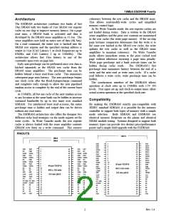
PINOUTS
1Mx16
4Mx4
2Mx8
VDD
DQ0
1
50
49
48
47
46
45
44
43
42
41
40
VSS
2
DQ15
DQ14
VSSQ
DQ13
DQ12
VDDQ
DQ11
DQ10
VSSQ
DQ9
DQ1
3
VDD
NC
VDD
1
2
3
4
5
6
7
8
9
44
43
42
41
40
39
38
37
36
VSS
DQ7
VSS
NC
VSSQ
DQ2
4
DQ0
5
VSSQ
DQ0
VSSQ
DQ1
VSSQ VSSQ
DQ6 DQ3
VDDQ VDDQ
DQ5 NC
VSSQ VSSQ
DQ4 DQ2
VDDQ VDDQ
DQ3
6
VDDQ
DQ4
7
VDDQ
NC
VDDQ
DQ2
8
DQ5
9
VSSQ
DQ1
VSSQ
DQ3
VSSQ
DQ6
10
11
50 pin TSOP-II
400 x 825 mils
0.8 mm pitch
VDDQ
VDDQ
44 pin TSOP-II
400 x 725 mils
0.8 mm pitch
DQ7
12
13
39
38
DQ8
NC
NC
10
11
12
13
35
34
33
32
NC
NC
VDDQ
VDDQ
NC
NC
NC
NC
LDQM
/WE
14
15
37
36
NC
/WE
/CAS
/WE
/CAS
DQM
CLK
DQM
CLK
UDQM
/CAS
/RAS
/CS
16
17
18
19
20
21
22
23
24
25
35
34
33
32
31
30
29
28
27
26
CLK
CKE
NC
A9
/RAS
/CS
/RAS
/CS
14
15
16
17
18
19
20
21
22
31
30
29
28
27
26
25
24
23
CKE
NC
A9
CKE
NC
A9
A11 (BS) A11 (BS)
A10/AP A10/AP
A11 (BS)
A10/AP
A0
A8
A8
A8
A0
A0
A7
A7
A7
A1
A1
A6
A6
A1
A6
A2
A2
A5
A5
A2
A5
A3
A3
A4
A4
A3
A4
VDD
VDD
VSS
VSS
VDD
VSS
Rev. 2.4
2

 RAMTRON [ RAMTRON INTERNATIONAL CORPORATION ]