16Mbit ESDRAM Family
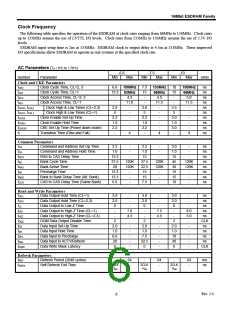
Clock Frequency and Latency (-6.6ns Speed Bin)
Clock Frequency (MHz)
Symbol
tCK
Parameter
Clock Cycle Time
66
15
1
75
13.3
1
100
10
2
133
7.5
2
150
6.6
2
Units
ns
CAS Latency
tAA
tCK
tCK
tCK
tCK
tCK
tCK
tCK
tCK
tCK
tCK
RAS to CAS Delay
RAS Latency
1
1
2
2
2
tRCD
tRL
2
2
4
4
4
Bank Cycle Time
3
3
4
5
6
tRC
Minimum Bank Active Time
Precharge Time
2
2
3
3
3
tRAS
tRP
1
1
2
2
2
Data-In to Precharge Time
Data-In to Active/Refresh
Bank to Bank Delay Time
CAS to CAS Delay Time
1
1
1
1
1
tDPL
tDAL
tRRD
tCCD
2
2
3
3
3
1
1
2
2
2
1
1
1
1
1
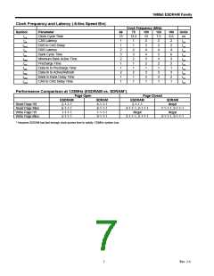
Performance Comparison at 133MHz (ESDRAM vs. SDRAM*)
Page Open
Page Closed
ESDRAM
2-1-1-1
6-1-1-1
1-1-1-1
5-1-1-1
SDRAM
4-1-1-1
8-1-1-1
1-1-1-1
9-1-1-1
ESDRAM
2-1-1-1
4-1-1-1, 2-1-1-1
illegal
SDRAM
illegal
7-1-1-1, 9-1-1-1
illegal
3-1-1-1, 9-1-1-1
Read Page Hit
Read Page Miss
Write Page Hit
Write Page Miss
2-1-1-1, 5-1-1-1
* Assumes SDRAM has fast enough clock access time to satisfy 133MHz system bus.
Rev. 2.4
7

 RAMTRON [ RAMTRON INTERNATIONAL CORPORATION ]