FM24CL64B - 64Kb 3V I2C F-RAM (Automotive Temp.)
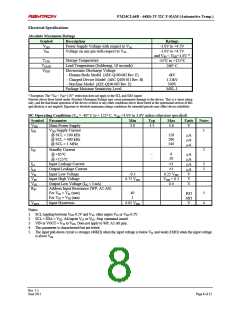
AC Parameters (TA = -40 C to + 125 C, VDD =3.0V to 3.6V unless otherwise specified)
Symbol Parameter Min Max Min Max Min Max Units Notes
fSCL
tLOW
tHIGH
tAA
SCL Clock Frequency
Clock Low Period
Clock High Period
SCL Low to SDA Data Out Valid
0
4.7
4.0
100
0
1.3
0.6
400
0
0.6
0.4
1000
kHz
s
s
1
3
0.9
0.55
s
tBUF
Bus Free Before New
Transmission
4.7
1.3
0.5
s
tHD:STA
tSU:STA
Start Condition Hold Time
Start Condition Setup for Repeated
Start
4.0
4.7
0.6
0.6
0.25
0.25
s
s
tHD:DAT
tSU:DAT
tR
tF
tSU:STO
tDH
Data In Hold
Data In Setup
Input Rise Time
Input Fall Time
Stop Condition Setup
Data Output Hold
0
250
0
100
0
100
ns
ns
ns
ns
s
ns
1000
300
300
300
300
100
2
2
4.0
0
0.6
0
0.25
0
(from SCL @ VIL)
tSP
Noise Suppression Time Constant
on SCL, SDA
50
50
50
ns
Notes: All SCL specifications as well as start and stop conditions apply to both read and write operations.
1. The speed-related specifications are guaranteed characteristic points along a continuous curve of operation from DC to fSCL
(max).
2. This parameter is periodically sampled and not 100% tested.
Capacitance (TA = 25 C, f=1.0 MHz, VDD = 3.3V)
Symbol Parameter
Min
Max
Units Notes
CI/O
CIN
Input/Output Capacitance (SDA)
Input Capacitance
-
-
8
6
pF
pF
1
1
Notes
1. This parameter is periodically sampled and not 100% tested.
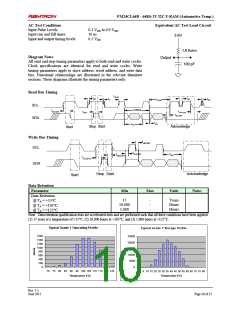
Power Cycle Timing
VDD min.
VDD
tVR
tVF
tPD
tPU
SDA,SCL
Power Cycle Timing (TA = -40 C to +125 C, VDD = 3.0V to 3.6V)
Symbol Parameter
Min
Max
Units Notes
ms
tPU
tPD
tVR
Power Up (VDD min) to First Access (Start condition)
Last Access (Stop condition) to Power Down (VDD min)
VDD Rise Time
10
0
30
100
-
-
-
-
s
s/V
s/V
1
1
tVF
VDD Fall Time
Notes
1. Slope measured at any point on VDD waveform.
Rev. 1.1
June 2011
Page 9 of 12

 RAMTRON [ RAMTRON INTERNATIONAL CORPORATION ]