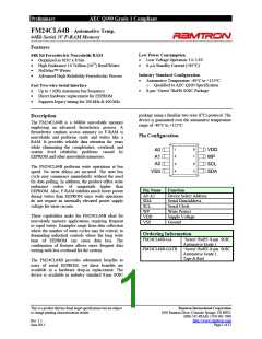
FM24CL64B - 64Kb 3V I2C F-RAM (Automotive Temp.)
configuration EEPROM during writes. The complete
operation for both writes and reads is explained
below.
Addressing Overview
After the FM24CL64B (as receiver) acknowledges
the slave address, the master can place the memory
address on the bus for a write operation. The address
requires two bytes. The first is the MSB. Since the
device uses only 13 address bits, the value of the
upper three bits are “don‟t care”. Following the MSB
is the LSB with the remaining eight address bits. The
address value is latched internally. Each access
causes the latched address value to be incremented
automatically. The current address is the value that is
held in the latch -- either a newly written value or the
address following the last access. The current address
will be held for as long as power remains or until a
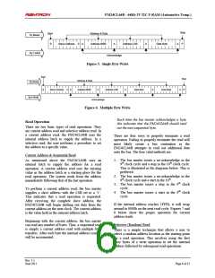
new value is written. Reads always use the current
address. A random read address can be loaded by
beginning a write operation as explained below.
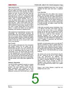
Write Operation
All writes begin with a slave address, then a memory
address. The bus master indicates a write operation
by setting the LSB of the slave address (R/W bit) to a
„0‟. After addressing, the bus master sends each byte
of data to the memory and the memory generates an
acknowledge condition. Any number of sequential
bytes may be written. If the end of the address range
is reached internally, the address counter will wrap
from 1FFFh to 0000h.
Unlike other nonvolatile memory technologies, there
is no effective write delay with F-RAM. Since the
read and write access times of the underlying
memory are the same, the user experiences no delay
through the bus. The entire memory cycle occurs in
less time than a single bus clock. Therefore, any
operation including read or write can occur
immediately following a write. Acknowledge polling,
a technique used with EEPROMs to determine if a
write is complete is unnecessary and will always
return a ready condition.
After transmission of each data byte, just prior to the
acknowledge, the FM24CL64B increments the
internal address latch. This allows the next sequential
byte to be accessed with no additional addressing.
After the last address (1FFFh) is reached, the address
latch will roll over to 0000h. There is no limit to the
number of bytes that can be accessed with a single
read or write operation.
Internally, an actual memory write occurs after the 8th
data bit is transferred. It will be complete before the
acknowledge is sent. Therefore, if the user desires to
abort a write without altering the memory contents,
this should be done using start or stop condition prior
to the 8th data bit. The FM24CL64B uses no page
buffering.
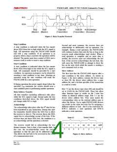
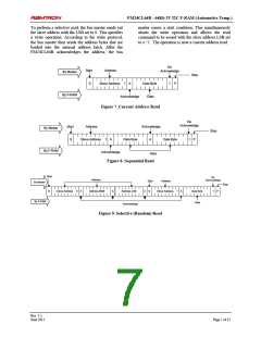
Data Transfer
After the address information has been transmitted,
data transfer between the bus master and the
FM24CL64B can begin. For a read operation the
FM24CL64B will place 8 data bits on the bus then
wait for an acknowledge from the master. If the
acknowledge occurs, the FM24CL64B will transfer
the next sequential byte. If the acknowledge is not
sent, the FM24CL64B will end the read operation.
For a write operation, the FM24CL64B will accept 8
data bits from the master then send an acknowledge.
All data transfer occurs MSB (most significant bit)
first.
The memory array can be write-protected using the
WP pin. Setting the WP pin to a high condition
(VDD
)
will write-protect all addresses. The
FM24CL64B will not acknowledge data bytes that
are written to protected addresses. In addition, the
address counter will not increment if writes are
attempted to these addresses. Setting WP to a low
state (VSS) will deactivate this feature. WP is pulled
down internally.
Memory Operation
The FM24CL64B is designed to operate in a manner
very similar to other 2-wire interface memory
products. The major differences result from the
higher performance write capability of F-RAM
technology. These improvements result in some
differences between the FM24CL64B and a similar
Figures 5 and 6 below illustrate a single-byte and
multiple-byte write cycles.
Rev. 1.1
June 2011
Page 5 of 12

 RAMTRON [ RAMTRON INTERNATIONAL CORPORATION ]