FM24CL64B - 64Kb 3V I2C F-RAM (Automotive Temp.)
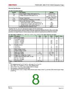
Equivalent AC Test Load Circuit
AC Test Conditions
Input Pulse Levels
0.1 VDD to 0.9 VDD
Input rise and fall times
Input and output timing levels
10 ns
0.5 VDD
3.6V
1.8 Kohm
Output
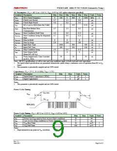
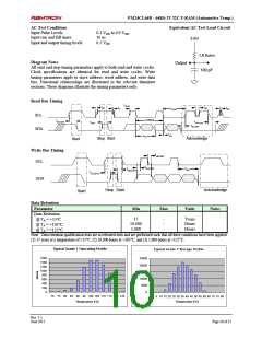
Diagram Notes
All start and stop timing parameters apply to both read and write cycles.
Clock specifications are identical for read and write cycles. Write
timing parameters apply to slave address, word address, and write data
bits. Functional relationships are illustrated in the relevant datasheet
sections. These diagrams illustrate the timing parameters only.
100 pF
Read Bus Timing
tHIGH
tR
tSP
tF
tSP
tLOW
`
SCL
1/fSCL
tSU:SDA
tHD:DAT
tSU:DAT
tBUF
SDA
tDH
tAA
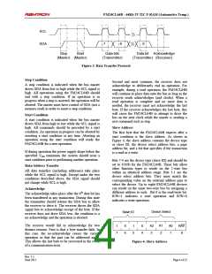
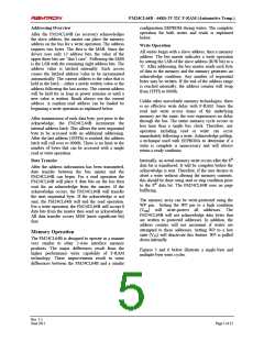
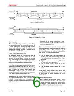
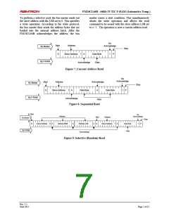
Stop Start
Acknowledge
Start
Write Bus Timing
tHD:DAT
SCL
tSU:DAT
tAA
tHD:STA
tSU:STO
SDA
Stop Start
Acknowledge
Start
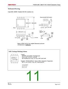
Data Retention
Parameter
Min
Max
Units
Notes
Data Retention
@ TA = +55C
@ TA = +105C
@ TA = +125C
17
10,000
1,000
-
-
-
Years
Hours
Hours
Note: Data retention qualification tests are accelerated tests and are performed such that all three conditions have been applied:
(1) 17 years at a temperature of +55C, (2) 10,000 hours at +105C, and (3) 1,000 hours at +125C.
Typical Grade 1 Operating Profile
Typical Grade 1 Storage Profile
1600
1400
1200
1000
800
600
400
200
0
25000
20000
15000
10000
5000
0
70 75 80 85 90 95 100 105 110 115 120 125
0
5
10 15 20 25 30 35 40 45 50 55 60 65 70 75 80
Temperature (°C)
Temperature (°C)
Rev. 1.1
June 2011
Page 10 of 12

 RAMTRON [ RAMTRON INTERNATIONAL CORPORATION ]