FM24CL64B - 64Kb 3V I2C F-RAM (Automotive Temp.)
Electrical Specifications
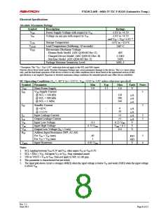
Absolute Maximum Ratings
Symbol
VDD
VIN
Description
Power Supply Voltage with respect to VSS
Voltage on any pin with respect to VSS
Ratings
-1.0V to +4.5V
-1.0V to +4.5V
and VIN < VDD+1.0V *
TSTG
TLEAD
VESD
Storage Temperature
Lead Temperature (Soldering, 10 seconds)
Electrostatic Discharge Voltage
-55C to +125C
260 C
- Human Body Model (AEC-Q100-002 Rev. E)
- Charged Device Model (AEC-Q100-011 Rev. B)
- Machine Model (AEC-Q100-003 Rev. E)
Package Moisture Sensitivity Level
4kV
1.25kV
300V
MSL-1
* Exception: The “VIN < VDD+1.0V” restriction does not apply to the SCL and SDA inputs.
Stresses above those listed under Absolute Maximum Ratings may cause permanent damage to the device. This is a stress rating
only, and the functional operation of the device at these or any other conditions above those listed in the operational section of this
specification is not implied. Exposure to absolute maximum ratings conditions for extended periods may affect device reliability.
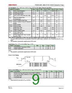
DC Operating Conditions (TA = -40 C to + 125 C, VDD =3.0V to 3.6V unless otherwise specified)
Symbol Parameter
Min
Typ
Max
Units
Notes
VDD
IDD
Main Power Supply
3.0
3.3
3.6
V
VDD Supply Current
@ SCL = 100 kHz
@ SCL = 400 kHz
@ SCL = 1 MHz
1
120
200
340
A
A
A
ISB
Standby Current
@ +85C
@ +125C
Input Leakage Current
Output Leakage Current
Input Low Voltage
Input High Voltage
Output Low Voltage (IOL = 3 mA)
Address Input Resistance (WP, A2-A0)
For VIN = VIL (max)
2
-
-
6
20
A
A
A
A
V
ILI
±1
±1
0.25 VDD
VDD + 0.3
0.4
3
3
ILO
VIL
VIH
VOL
RIN
-0.3
0.75 VDD
V
V
40
1
5
4
K
M
V
For VIN = VIH (min)
VHYS
Input Hysteresis
0.05 VDD
Notes
1. SCL toggling between VDD-0.2V and VSS, other inputs VSS or VDD-0.2V.
2. SCL = SDA = VDD. All inputs VSS or VDD. Stop command issued.
3. VIN or VOUT = VSS to VDD. Does not apply to WP, A2-A0 pins.
4. This parameter is characterized but not tested.
5. The input pull-down circuit is stronger (40K) when the input voltage is below VIL and weak (1M) when the input voltage
is above VIH.
Rev. 1.1
June 2011
Page 8 of 12

 RAMTRON [ RAMTRON INTERNATIONAL CORPORATION ]