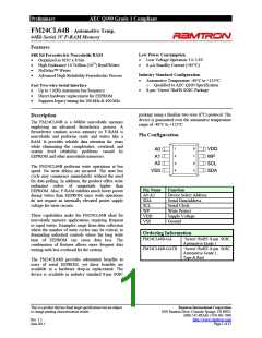
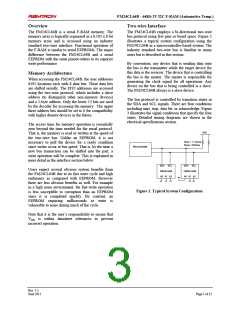
FM24CL64B - 64Kb 3V I2C F-RAM (Automotive Temp.)
Overview
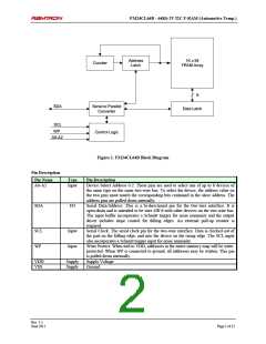
Two-wire Interface
The FM24CL64B is a serial F-RAM memory. The
memory array is logically organized as a 8,192 x 8 bit
memory array and is accessed using an industry
standard two-wire interface. Functional operation of
the F-RAM is similar to serial EEPROMs. The major
difference between the FM24CL64B and a serial
EEPROM with the same pinout relates to its superior
write performance.
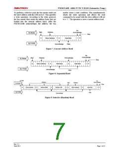
The FM24CL64B employs a bi-directional two-wire
bus protocol using few pins or board space. Figure 2
illustrates a typical system configuration using the
FM24CL64B in a microcontroller-based system. The
industry standard two-wire bus is familiar to many
users but is described in this section.
By convention, any device that is sending data onto
the bus is the transmitter while the target device for
this data is the receiver. The device that is controlling
the bus is the master. The master is responsible for
generating the clock signal for all operations. Any
device on the bus that is being controlled is a slave.
The FM24CL64B always is a slave device.
Memory Architecture
When accessing the FM24CL64B, the user addresses
8192 locations each with 8 data bits. These data bits
are shifted serially. The 8192 addresses are accessed
using the two-wire protocol, which includes a slave
address (to distinguish other non-memory devices)
and a 2-byte address. Only the lower 13 bits are used
by the decoder for accessing the memory. The upper
three address bits should be set to 0 for compatibility
with higher density devices in the future.
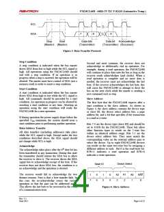
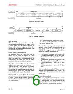
The bus protocol is controlled by transition states in
the SDA and SCL signals. There are four conditions
including start, stop, data bit, or acknowledge. Figure
3 illustrates the signal conditions that specify the four
states. Detailed timing diagrams are shown in the
electrical specifications section.
The access time for memory operation is essentially
zero beyond the time needed for the serial protocol.
That is, the memory is read or written at the speed of
the two-wire bus. Unlike an EEPROM, it is not
necessary to poll the device for a ready condition
since writes occur at bus speed. That is, by the time a
new bus transaction can be shifted into the part, a
write operation will be complete. This is explained in
more detail in the interface section below.
VDD
Rmin = 1.1 Kohm
Rmax = tR/Cbus
Microcontroller
SDA
SCL
SDA
SCL
Users expect several obvious system benefits from
the FM24CL64B due to its fast write cycle and high
endurance as compared with EEPROM. However
there are less obvious benefits as well. For example
in a high noise environment, the fast-write operation
is less susceptible to corruption than an EEPROM
since it is completed quickly. By contrast, an
EEPROM requiring milliseconds to write is
vulnerable to noise during much of the cycle.
FM24CL64B
A0 A1 A2
FM24CL64B
A0 A1 A2
Figure 2. Typical System Configuration
Note that it is the user‟s responsibility to ensure that
VDD is within datasheet tolerances to prevent
incorrect operation.
Rev. 1.1
June 2011
Page 3 of 12

 RAMTRON [ RAMTRON INTERNATIONAL CORPORATION ]