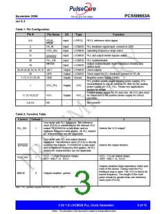
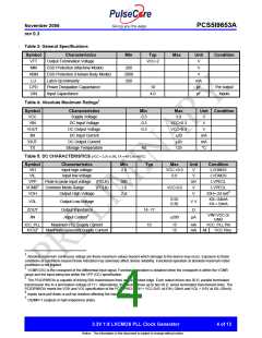
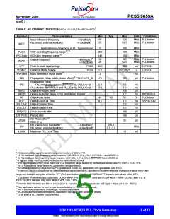
November 2006
PCS5I9653A
rev 0.3
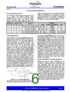
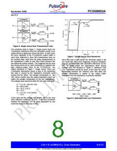
Calculation of part-to-part skew
resulting in a worst case timing uncertainty from input to
any output of -197 pS to 297 pS (at 125MHz reference
frequency) relative to PCLK:
The PCS5I9653A zero delay buffer supports applications
where critical clock signal timing can be maintained
across several devices. If the reference clock inputs of
two or more PCS5I9653A are connected together, the
maximum overall timing uncertainty from the common
PCLK input to any output is: tSK(PP) = t(Ø) + tSK(O) +
tPD, LINE(FB) + tJIT(Ø) ¡ CF This maximum timing
uncertainty consist of 4 components: static phase offset,
output skew, feedback board trace delay and I/O (phase)
jitter:
tSK(PP) = [-17pS...117pS] + [-150pS...150pS] +
[(10pS . -3)...(10pS . 3)] + tPD, LINE(FB)
tSK(PP) = [-197pS...297pS] + tPD, LINE(FB)
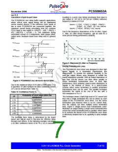
Due to the frequency dependence of the I/O jitter, Figure
5. .Max. I/O Jitter versus frequency. can be used for a
more precise timing performance analysis.
Figure 5. Maximum I/O Jitter vs Frequency
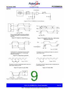
Driving Transmission Lines
The PCS5I9653A clock driver was designed to drive high
speed signals in
a
terminated transmission line
environment. To provide the optimum flexibility to the
user the output drivers were designed to exhibit the
lowest impedance possible. With an output impedance of
less than 20ꢀ the drivers can drive either parallel or
series terminated transmission lines. In most high
performance clock networks point-to-point distribution of
signals is the method of choice. In a point-to-point
scheme either series terminated or parallel terminated
transmission lines can be used. The parallel technique
terminates the signal at the end of the line with a
50ꢀ resistance to VCC÷2.
Figure 4. PCS5I9653A max device-to-device skew
Due to the statistical nature of I/O jitter a RMS value (1 σ)
is specified. I/O jitter numbers for other confidence factors
(CF) can be derived from Table 10.
Table 10: Confidence Factor CF
Probability of clock edge within the
CF
This technique draws a fairly high level of DC current and
thus only a single terminated line can be driven by each
output of the PCS5I9653A clock driver. For the series
terminated case however there is no DC current draw,
thus the outputs can drive multiple series terminated
lines. Figure 6 “Single versus Dual Transmission Lines”
Illustrates an output driving a single series terminated line
versus two series terminated lines in parallel. When taken
to its extreme the fanout of the PCS5I9653A clock driver
is effectively doubled due to its capability to drive multiple
lines.
distribution
± 1σ
± 2σ
± 3σ
± 4σ
± 5σ
± 6σ
0.68268948
0.95449988
0.99730007
0.99993663
0.99999943
0.99999999
The feedback trace delay is determined by the board
layout and can be used to fine-tune the effective delay
through each device. In the following example calculation
a I/O jitter confidence factor of 99.7% (± 3σ) is assumed,
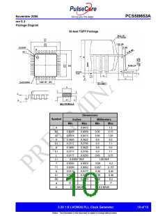
3.3V 1:8 LVCMOS PLL Clock Generator
7 of 13
Notice: The information in this document is subject to change without notice.

 PULSECORE [ PulseCore Semiconductor ]