November 2006
rev 0.3
PCS5I9653A
APPLICATIONS INFORMATION
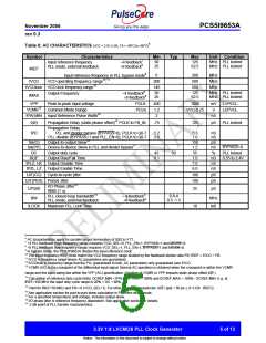
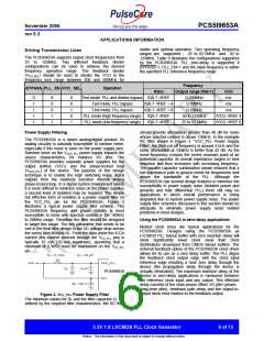
stable and optimal operation. Two operating frequency
ranges are supported : 25 to 62.5MHz and 50 to
125MHz. Table 9 illustrates the configurations supported
by the PCS5I9653A. PLL zero-delay is supported if
BYPASS=1, PLL_EN=1 and the input frequency is within
the specified PLL reference frequency range.
Driving Transmission Lines
The PCS5I9653A supports output clock frequencies from
25 to 125MHz. Two different feedback divider
configurations can be used to achieve the desired
frequency operation range. The feedback divider
(VCO_SEL) should be used to situate the VCO in the
frequency lock range between 200 and 500MHz for
Frequency
Output range (fQ0-7)
0-200MHz
BYPASS PLL_ EN VCO_ SEL
Operation
Ratio
VCO
n/a
n/a
0
1
1
1
1
X
0
0
1
1
X
0
1
0
1
Test mode: PLL and divider bypass fQ0-7 =fREF
Test mode: PLL bypass
Test mode: PLL bypass
PLL mode (high frequency range)
PLL mode (low frequency range)
fQ0-7 =fREF ÷ 4
fQ0-7 =fREF ÷ 8
fQ0-7 =fREF
0-50MHz
0-25MHz
50 to 125MHz
25 to 62.5MHz
n/a
fVCO =fREF 4
fVCO =fREF 8
fQ0-7 =fREF
Power Supply Filtering
should provide attenuation greater than 40 dB for noise
whose spectral content is above 100kHz. In the example
RC filter shown in Figure 3. “VCC_PLL Power Supply
Filter”, the filter cut-off frequency is around 4 kHz and the
noise attenuation at 100kHz is better than 42 dB. As the
noise frequency crosses the series resonant point of an
individual capacitor its overall impedance begins to look
inductive and thus increases with increasing frequency.
The parallel capacitor combination shown ensures that a
low impedance path to ground exists for frequencies well
above the bandwidth of the PLL. Although the
PCS5I9653A has several design features to minimize the
susceptibility to power supply noise (isolated power and
grounds and fully differential PLL) there still may be
applications in which overall performance is being
degraded due to system power supply noise. The power
supply filter schemes discussed in this section should be
adequate to eliminate power supply noise related
problems in most designs.
The PCS5I9653A is a mixed analog/digital product. Its
analog circuitry is naturally susceptible to random noise,
especially if this noise is seen on the power supply pins.
Random noise on the VCCA_PLL power supply impacts the
device characteristics, for instance I/O jitter. The
PCS5I9653A provides separate power supplies for the
output buffers (VCC) and the phase-locked loop
(VCCA_PLL) of the device. The purpose of this design
technique is to isolate the high switching noise digital
outputs from the relatively sensitive internal analog
phase-locked loop. In a digital system environment where
it is more difficult to minimize noise on the power supplies
a second level of isolation may be required. The simple
but effective form of isolation is a power supply filter on
the VCC_PLL pin for the PCS5I9653A. Figure
3
illustrates a typical power supply filter scheme. The
PCS5I9653A frequency and phase stability is most
susceptible to noise with spectral content in the 100kHz
to 20MHz range. Therefore the filter should be designed
to target this range. The key parameter that needs to be
met in the final filter design is the DC voltage drop across
the series filter resistor RF. From the data sheet the ICCA
current (the current sourced through the VCC_PLL pin) is
typically 10 mA (15 mA maximum), assuming that a
minimum of 2.985V must be maintained on the VCC_PLL
pin.
Using the PCS5I9653A in zero-delay applications
Nested clock trees are typical applications for the
PCS5I9653A. Designs using the PCS5I9653A as
LVCMOS PLL fanout buffer with zero insertion delay will
show significantly lower clock skew than clock
distributions developed from CMOS fanout buffers. The
external feedback option of the PCS5I9653A clock driver
allows for its use as a zero delay buffer. The PLL aligns
the feedback clock output edge with the clock input
reference edge resulting a near zero delay through the
device (the propagation delay through the device is
virtually eliminated). The maximum insertion delay of the
device in zero-delay applications is measured between
the reference clock input and any output. This effective
delay consists of the static phase offset, I/O jitter (phase
long-term jitter), feedback path delay and the output-to-
output skew error relative to the feedback output.
PCS5I9653A
Figure 3. VCC_PLL Power Supply Filter
The minimum values for RF and the filter capacitor CF are
defined by the required filter characteristics: the RC filter
3.3V 1:8 LVCMOS PLL Clock Generator
6 of 13
Notice: The information in this document is subject to change without notice.

 PULSECORE [ PulseCore Semiconductor ]