November 2006
rev 0.3
PCS5I9653A
PCS5I9653A
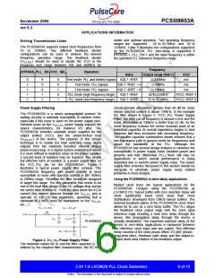
OUTPUT BUFFER
Z0=15ꢀ
RS=36ꢀ
IN
IN
14ꢀ
OUTA
PCS5I9653A
Z0=15ꢀ
Z0=15ꢀ
RS=36ꢀ
RS=36ꢀ
OUTPUT BUFFER
OUTB0
OUTB1
14ꢀ
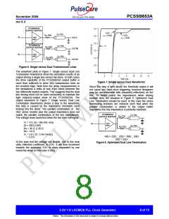
Figure 6. Single versus Dual Transmission Lines
The waveform plots in Figure 7 .Single versus Dual Line
Termination Waveforms show the simulation results of an
output driving a single line versus two lines. In both cases
the drive capability of the PCS5I9653A output buffer is
more than sufficient to drive 50ꢀ transmission lines on
the incident edge. Note from the delay measurements in
the simulations a delta of only 43ps exists between the
two differently loaded outputs. This suggests that the dual
line driving need not be used exclusively to maintain the
tight output-to-output skew of the PCS5I9653A. The
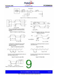
output waveform in Figure 7 Single versus Dual Line
Termination Waveforms shows a step in the waveform,
this step is caused by the impedance mismatch seen
looking into the driver. The parallel combination of the
36ꢀ series resistor plus the output impedance does not
match the parallel combination of the line impedances.
The voltage wave launched down the two lines will equal:
Figure 7. Single versus Dual Waveforms
Since this step is well above the threshold region it will
not cause any false clock triggering, however designers
may be uncomfortable with unwanted reflections on the
line. To better match the impedances when driving
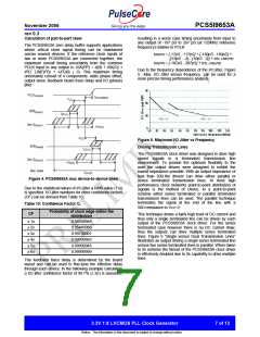
multiple lines the situation in Figure 8 .Optimized Dual
Line Termination should be used. In this case the series
terminating resistors are reduced such that when the
parallel combination is added to the output buffer
impedance the line impedance is perfectly matched.
PCS5I9653A
Z0=15ꢀ
RS=22ꢀ
OUTPUT BUFFER
VL = VS ( Z0 ÷ (RS+R0 +Z0))
Z0 = 50ꢀ || 50ꢀ
14ꢀ
IN
Z0=15ꢀ
RS=22ꢀ
RS = 36 ꢀ || 36 ꢀ
R0 = 14 ꢀ
VL==13.3.01V( 25 (18+14+25)
14Ω + 22Ω _ 22Ω = 50Ω _ 50Ω
25Ω = 25Ω
At the load end the voltage will double, due to the near
unity reflection coefficient, to 2.6V. It will then increment
towards the quiescent 3.0V in steps separated by one
round trip delay (in this case 4.0nS).
Figure 8. Optimized Dual Line Termination
3.3V 1:8 LVCMOS PLL Clock Generator
8 of 13
Notice: The information in this document is subject to change without notice.

 PULSECORE [ PulseCore Semiconductor ]