November 2006
rev 0.3
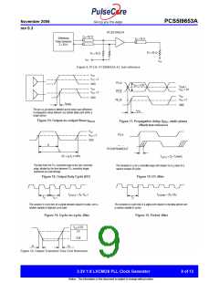
PCS5I9653A
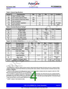
Table 3: General Specifications
Symbol
VTT
MM
HBM
LU
Characteristics
Min
Typ
VCC÷2
Max
Unit
V
V
Condition
Output Termination Voltage
ESD Protection (Machine Model)
ESD Protection (Human Body Model)
Latch-Up Immunity
Power Dissipation Capacitance
Input Capacitance
200
2000
200
V
mA
pF
pF
CPD
CIN
10
4.0
Per output
Inputs
Table 4: Absolute Maximum Ratings1
Symbol
VCC
VIN
VOUT
IIN
Characteristics
Supply Voltage
Min
Max
3.9
VCC+0.3
VCC+0.3
±20
Unit Condition
-0.3
-0.3
-0.3
V
V
DC Input Voltage
DC Output Voltage
DC Input Current
DC Output Current
Storage Temperature
V
mA
mA
°C
IOUT
TS
±50
125
-65
Table 5: DC CHARACTERISTICS (VCC = 3.3V ± 5%, TA =-40°C to +85°C)
Symbol
VIH
Characteristics
Input high voltage
Input low voltage
Min
Typ
Max
VCC +0.3
0.8
Unit
V
V
mV
V
V
Condition
LVCMOS
LVCMOS
LVPECL
2.0
VIL
VPP
Peak-to-peak input voltage (PCLK)
Common Mode Range
Output High Voltage
300
1.0
2.4
VCMR2
VOH
(PCLK)
VCC-0.6
LVPECL
IOH=-24 mA3
0.55
0.30
IOL=24mA
VOL
Output Low Voltage
V V
IOL=12mA
ZOUT
IIN
Output impedance
Input Current4
14 -17
10
Ω
VIN=VCC or
GND
±200
µA
ICC_PLL
ICCQ5
Maximum PLL Supply Current
Maximum Quiescent Supply Current
15
15
mA
mA
VCC_PLL Pin
All
VCC Pins
1
Absolute maximum continuous ratings are those maximum values beyond which damage to the device may occur. Exposure to these
conditions or conditions beyond those indicated may adversely affect device reliability. Functional operation at absolute-maximum-rated
conditions is not implied.
2
VCMR (DC) is the crosspoint of the differential input signal. Functional operation is obtained when the crosspoint is within the VCMR
range and the input swing lies within the VPP (DC) specification.
3
The PCS3P9653A is capable of driving 50ꢀ transmission lines on the incident edge. Each output drives one 50 ꢀ parallel terminated
transmission line to a termination voltage of VTT. Alternatively, the device drives up to two 50 ꢀ series terminated transmission lines. The
PCS3P9653A meets the VOH and VOL specification of the PCS3P953 (VOH > VCC-0.6V at IOH=-20mA and VOL > 0.6V at IOL=20mA).
4
Inputs have pull-down or pull-up resistors affecting the input current.
5
OE/MR=1 (outputs in high-impedance state).
3.3V 1:8 LVCMOS PLL Clock Generator
4 of 13
Notice: The information in this document is subject to change without notice.

 PULSECORE [ PulseCore Semiconductor ]