November 2006
rev 0.3
PCS5I9653A
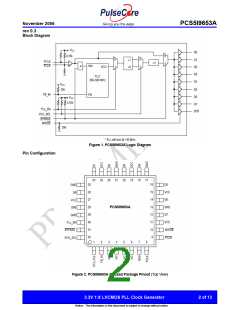
Table 1: Pin Configuration
Pin #
Pin Name
I/O
Type
Function
8,9
PCLK,
PCLK
Input
LVPECL
PECL reference clock signal
2
32
FB_IN
VCO_SEL
Input
Input
LVCMOS PLL feedback signal input, connect to QFB
LVCMOS Operating frequency range select
31
30
10
Input
Input
Input
LVCMOS PLL and output divider bypass select
LVCMOS PLL enable/disable
BYPASS
PLL_EN
MR/OE
Output enable/disable (high-impedance tristate) and
LVCMOS
device reset
26,24,22,20,18,16,14,12 Q0-7
Output LVCMOS Clock outputs
28
QFB
GND
Output LVCMOS Clock output for PLL feedback, connect to FB_IN
7,13,17,21,25,29
Supply Ground
Negative power supply (GND)
PLL positive power supply (analog power supply). It is
recommended to use an external RC filter for the analog
power supply pin VCC_PLL. Please see applications
section for details
1
VCC_PLL
Supply
VCC
Positive power supply for I/O and core. All VCC pins must
be connected to the positive power supply for correct
operation
11,15,19,23,27
3,4,5,6
VCC
NC
Supply
-
VCC
-
No Connect
Table 2: Function Table
Control Default
0
1
Test mode with PLL bypassed. The reference
clock (PCLK) is substituted for the internal VCO
output. PCS5I9653A is fully static and no
minimum frequency limit applies. All PLL related
AC characteristics are not applicable.
PLL_EN
1
Selects the VCO output1
Test mode with PLL and output dividers
bypassed. The reference clock (PCLK) is directly
routed to the outputs. PCS5I9653A is fully static
and no minimum frequency limit applies. All PLL
related AC characteristics are not applicable.
1
1
Selects the output dividers.
BYPASS
VCO ÷ 1 (High frequency range).
fREF =fQ0-7 =4 . fVCO
VCO ÷ 2 (Low output range).
fREF =fQ0-7 =8 . fVCO
VCO_SEL
Outputs disabled (high-impedance state) and
reset of the device. During reset the PLL
feedback loop is open. The VCO is tied to its
lowest frequency. The length of the reset
pulse should be greater than one reference
clock cycle (PCLK).
MR/OE
0
Outputs enabled (active)
Note: 1 PLL operation requires BYPASS=1 and PLL_EN=1.
3.3V 1:8 LVCMOS PLL Clock Generator
3 of 13
Notice: The information in this document is subject to change without notice.

 PULSECORE [ PulseCore Semiconductor ]