November 2006
rev 0.3
PCS5I9653A
6
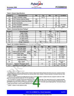
Table 6: AC CHARACTERISTICS (VCC = 3.3V ± 5%, TA = -40°C to +85°C)
Symbol
fREF
Characteristics
Min
50
Typ
Max
125
Unit Condition
MHz PLL locked
MHz PLL locked
Input reference frequency
PLL mode, external feedback
÷4 feedback7
÷8 feedback8
25
62.5
Input reference frequency in PLL bypass mode9
0
200
145
200
500
500
MHz
MHz
MHz
fVCO
VCO operating frequency range10,11
fVCOlock VCO lock frequency range12
Output Frequency
÷4 feedback8
÷8 feedback9
50
125
MHz PLL locked
fMAX
25
62.5
MHz PLL locked
VPP
Peak-to-peak input voltage
Common Mode Range
PCLK
PCLK
450
1.2
2
1000
VCC-0.75
mV
V
nS
LVPECL
LEPVCL
VCMR13
tPW,MIN Input Reference Pulse Width14
Propagation Delay (static phase offset)15 PCLK to FB_IN
-75
125
pS
PLL locked
t(Ø)
Propagation Delay
tPD
PLL and divider bypass (BYPASS=0), PCLK to Q0-7
PLL disable (BYPASS=1 and PLL_EN=0), PCLK to Q0-7
Output-to-output Skew16
1.2
3.0
3.3
7.0
150
1.5
nS
nS
pS
nS
tsk(O)
tsk(PP)
Device-to-device Skew in PLL and divider bypass17
BYPASS=0
PLL locked
0.55 to 2.4V
DC
Output duty cycle
45
0.1
50
55
1.0
7.0
%
tR,tF
Output Rise/Fall Time
nS
tPLZ, HZ Output Disable Time
nS
tPZL, LZ
tJIT(CC)
tJIT(PER) Period Jitter
Output Enable Time
Cycle-to-cycle jitter
6.0
100
100
nS
pS
pS
I/O Phase Jitter18
25
pS
tJIT(Ø)
RMS (1 σ)
PLL closed loop bandwidth19
PLL mode, external feedback
÷ 4 feedback8
÷8 feedback9
0.8-4
BW
MHz
mS
0.5 -1.3
tLOCK
Maximum PLL Lock Time
10
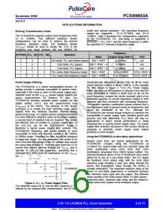
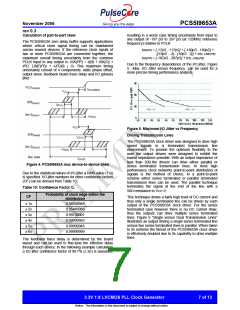
6 AC characteristics apply for parallel output termination of 50ꢀ to VTT.
7 ÷4 PLL feedback (high frequency range) requires VCO_SEL=0, PLL_EN=1, BYPASS=1 and MR/OE=0.
8 ÷8 PLL feedback (low frequency range) requires VCO_SEL=1, PLL_EN=1, BYPASS=1 and MR/OE=0.
9 In bypass mode, the PCS3P9653A divides the input reference clock.
10 The input frequency fREF must match the VCO frequency range divided by the feedback divider ratio FB: fREF = fVCO ÷ FB.
11 fVCO is frequency range where AC parameters are guaranteed.
12 fVCOlock is frequency range that the PLL guaranteed to lock, AC parameters only guaranteed over fVCO.
13 VCMR (AC) is the crosspoint of the differential input signal. Normal AC operation is obtained when the crosspoint is within the VCMR
range and the input swing lies within the VPP (AC) specification. Violation of VCMR or VPP impacts static phase offset t(Ø ).
14 Calculation of reference duty cycle limits: DCREF,MIN = tPW,MIN . fREF . 100% and DCREF,MAX = 100% - DCREF,MIN. E.g. at
fREF=100 MHz the input duty cycle range is 20% < DC < 80%.
15 Valid for fREF=50 MHz and FB=÷8 (VCO_SEL=1). For other reference frequencies: t(Ø ) [ps] = 50 ps ± (1÷(120 . fREF)).
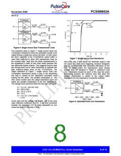
16 See application section for part-to-part skew calculation in PLL zero-delay mode.
17 For a specified temperature and voltage, includes output skew.
18 I/O phase jitter is reference frequency dependent. See application section for details.
19 -3 dB point of PLL transfer characteristics.
3.3V 1:8 LVCMOS PLL Clock Generator
5 of 13
Notice: The information in this document is subject to change without notice.

 PULSECORE [ PulseCore Semiconductor ]