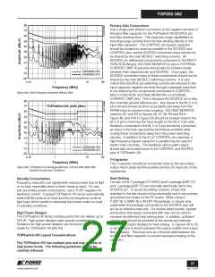
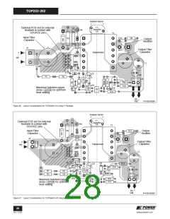
TOP252-262
Isolation Barrier
Y1-
Capacitor
C6
Optional PCB slot for external
heatsink in contact with
SOURCE pins
C2
R4
T1
Input Filter
Capacitor
C10
D3
R9
R3
Output
Rectifier
D1
J1
Output Filter
Capacitor
Transformer
+
C7
S
S
S
S
D
HV
U1
-
C
C1
L1
M
JP1
C4
C3
R8
C5
C8
R1
R2
J2
D2
R11
R10
U3
C9
R12
JP2
U2
Maximize hatched copper
areas (
) for optimum
VR2
heat sinking
DC
Out
-
+
PI-4753-070307
Figure 46. Layout Considerations for TOPSwitch-HX Using P-Package.
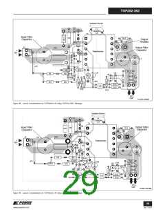
Isolation Barrier
C2
Optional PCB slot for external
heatsink in contact with
Y1-
Capacitor
C6
R6
T1
SOURCE pins
R5
Input Filter
Capacitor
Output
Rectifier
R12
J1
D1
Output Filter
Capacitor
+
D3
Transformer
HV
-
C7
D
S
S
U1
S
C
X
V
L1
C1
S
S
JP1
C4
R8
R7
C3
C9
C5
R13
R14
D2
C8
J2
U3
R15
R1
R3
R2
R4
R9
JP2
U2
VR2
R16
R17
Maximize hatched copper
areas (
) for optimum
heat sinking
-
+
DC
Out
PI-4752-070307
Figure 47. Layout Considerations for TOPSwitch-HX Using M-Package.
28
Rev. F 01/09
www.powerint.com

 POWERINT [ Power Integrations ]