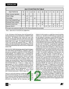
TOP242-249
secondresistorconnectedbetweentheEXTERNAL CURRENT
LIMIT (X) pin (Y or R package) or MULTI-FUNCTION (M)
pin (P or G package) and the rectified DC high voltage bus, the
current limit is reduced with increasing line voltage, allowing
a true power limiting operation against line variation to be
implemented. When using an RCD clamp, this power limiting
technique reduces maximum clamp voltage at high line. This
allows for higher reflected voltage designs as well as reducing
clamp dissipation.
40% of the initial UV threshold to allow extended input voltage
operating range (UV low threshold). If the UV low threshold
is reached during operation without the power supply losing
regulation the device will turn off and stay off until UV (high
threshold) has been reached again. If the power supply loses
regulation before reaching the UV low threshold, the device
will enter auto-restart. At the end ofeach auto-restart cycle (S7),
the UV comparator is enabled. If the UV high threshold is not
exceededtheMOSFETwillbedisabledduringthenextcycle(see
figure 8). The UV feature can be disabled independent of OV
feature as shown in Figure 19 and 23.
The leading edge blanking circuit inhibits the current limit
comparator for a short time after the output MOSFET is turned
on. The leading edge blanking time has been set so that, if a
power supply is designed properly, current spikes caused by
primary-side capacitances and secondary-side rectifier reverse
recovery time should not cause premature termination of the
switching pulse.
Line Overvoltage Shutdown (OV)
ThesameresistorusedforUValsosetsanovervoltagethreshold
which, once exceeded, will force TOPSwitch-GX output into
off-state. The ratio of OV and UV thresholds is preset at 4.5 as
canbeseeninFigure11. WhentheMOSFETisoff,therectified
DC high voltage surge capability is increased to the voltage
rating of the MOSFET (700 V), due to the absence of the
reflected voltage and leakage spikes on the drain. A small
amountofhysteresisisprovidedontheOVthresholdtoprevent
noise triggering. The OV feature can be disabled independent
of the UV feature as shown in Figure 18 and 32.
The current limit is lower for a short period after the leading
edge blanking time as shown in Figure 52. This is due to
dynamic characteristics of the MOSFET. To avoid triggering
thecurrentlimitinnormaloperation,thedraincurrentwaveform
should stay within the envelope shown.
Line Under-Voltage Detection (UV)
Line Feed Forward with DCMAX Reduction
At power up, UV keeps TOPSwitch-GX off until the input line
voltage reaches the under voltage threshold. At power down,
UV prevents auto-restart attempts after the output goes out of
regulation. This eliminates power down glitches caused by the
slow discharge of large input storage capacitor present in
applicationssuchasstandbysupplies.Asingleresistorconnected
from the LINE-SENSE pin (Y or R package) or MULTI-
FUNCTION pin (P or G package) to the rectified DC high
voltagebussetsUVthresholdduringpowerup. Oncethepower
supply is successfully turned on, the UV threshold is lowered to
The same resistor used for UV and OV also implements line
voltage feed forward which minimizes output line ripple and
reduces power supply output sensitivity to line transients. This
feed forward operation is illustrated in Figure 7 by the different
values of IL (Y or R package) or IM (P or G Package). Note that
for the same CONTROL pin current, higher line voltage results
in smaller operating duty cycle. As an added feature, the
maximumdutycycleDCMAX isalsoreducedfrom78%(typical)
at a voltage slightly higher than the UV threshold to 38%
(typical) at the OV threshold (see Figures 7, 11). Limiting
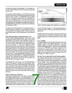
Oscillator
(SAW)
D
MAX
Enable from
X, L or M Pin (STOP)
Time
PI-2637-060600
Figure 10. Synchronization Timing Diagram.
E
7/01
August 8, 2000
8

 POWERINT [ Power Integrations ]