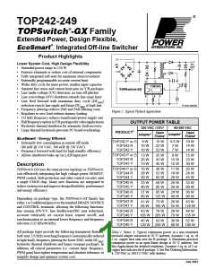
TOP242-249
TOPSwitch-GX Family Functional Description
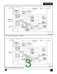
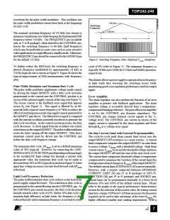
Like TOPSwitch, TOPSwitch-GX is an integrated switched
Auto-restart
ICD1
mode power supply chip that converts a current at the control
input to a duty cycle at the open drain output of a high voltage
powerMOSFET. Duringnormaloperationthedutycycleofthe
powerMOSFETdecreaseslinearlywithincreasingCONTROL
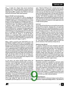
pin current as shown in Figure 7.
IB
I
= 125 µA
L
132
I
< I
L(DC)
L
I
= 190 µA
L
InadditiontothethreeterminalTOPSwitchfeatures,suchasthe
high voltage start-up, the cycle-by-cycle current limiting, loop
compensation circuitry, auto-restart, thermal shutdown, the
TOPSwitch-GX incorporates many additional functions that
reduce system cost, increase power supply performance and
design flexibility. A patented high voltage CMOS technology
allows both the high voltage power MOSFET and all the low
voltage control circuitry to be cost effectively integrated onto a
single monolithic chip.
30
IC (mA)
Auto-restart
ICD1
IB
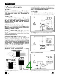
Three terminals, FREQUENCY, LINE-SENSE, and
EXTERNAL CURRENT LIMIT (available in Y or R package)
or one terminal MULTI-FUNCTION (available in P or G
Package) have been added to implement some of the new
functions. These terminals can be connected to the SOURCE
pin to operate the TOPSwitch-GX in a TOPSwitch-like three
terminal mode. However, even in this three terminal mode, the
TOPSwitch-GX offers many new transparent features that do
not require any external components:
78
Slope = PWM Gain
I
= 125 µA
L
38
10
I
< I
L(DC)
L
I
= 190 µA
L
TOP242/5 1.6 2.0
TOP246/9 2.2 2.6
5.2 6.0
5.8 6.6
1. A fully integrated 10 ms soft-start limits peak currents and
voltages during start-up and dramatically reduces or
eliminates output overshoot in most applications.
2. DCMAX of 78% allows smaller input storage capacitor, lower
input voltage requirement and/or higher power capability.
3. Frequency reduction at light loads lowers the switching
losses and maintains good cross regulation in multiple
output supplies.
4. Higher switching frequency of 132 kHz reduces the
transformer size with no noticeable impact on EMI.
5. Frequency jittering reduces EMI.
6. Hysteretic over-temperature shutdown ensures automatic
recoveryfromthermalfault.Largehysteresispreventscircuit
board overheating.
IC (mA)
Note: For P and G packages IL is replaced with IM.
PI-2633-060500
Figure 7. Relationship of Duty Cycle and Frequency to CONTROL
Pin Current.
The pin can also be used as a remote ON/OFF and a
synchronization input.
The EXTERNAL CURRENT LIMIT (X) pin is usually used to
reducethecurrentlimitexternallytoavalueclosetotheoperating
peak current, by connecting the pin to SOURCE through a
resistor. This pin can also be used as a remote ON/OFF and a
synchronization input in both modes. See Table 2 and Figure 11.
7. Packages with omitted pins and lead forming provide large
drain creepage distance.
For the P or G packages the LINE-SENSE and EXTERNAL
CURRENTLIMITpinfunctionsarecombinedononeMULTI-
FUNCTION (M) pin. However, some of the functions become
mutually exclusive as shown in Table 3.
8. Tighter absolute tolerances and smaller temperature vari-
ations on switching frequency, current limit and PWM gain.
The LINE-SENSE (L) pin is usually used for line sensing by
connecting a resistor from this pin to the rectified DC high
voltage bus to implement line overvoltage (OV), under-voltage
(UV) and line feed forward with DCMAX reduction. In this
mode,thevalueoftheresistordeterminestheOV/UVthresholds
and the DCMAX is reduced linearly starting from a line voltage
above the under-voltage threshold. See Table 2 and Figure 11.
The FREQUENCY (F) pin in the Y or R package sets the
switching frequency to the default value of 132 kHz when
connected to SOURCE pin. A half frequency option of 66 kHz
can be chosen by connecting this pin to CONTROL pin instead.
Leaving this pin open is not recommended.
E
7/01
August 8, 2000
5

 POWERINT [ Power Integrations ]