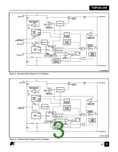
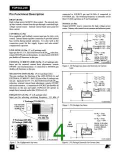
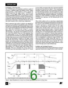
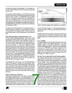
TOP242-249
CONTROL (C) Pin Operation
in excess of the consumption of the chip is shunted to SOURCE
through resistor RE as shown in Figure 2. This current flowing
through RE controls the duty cycle of the power MOSFET to
provide closed loop regulation. The shunt regulator has a finite
low output impedance ZC that sets the gain of the error amplifier
when used in a primary feedback configuration. The dynamic
impedance ZC of the CONTROL pin together with the external
CONTROL pin capacitance sets the dominant pole for the
control loop.
The CONTROL pin is a low impedance node that is capable of
receiving a combined supply and feedback current. During
normal operation, a shunt regulator is used to separate the
feedback signal from the supply current. CONTROL pin
voltage VC is the supply voltage for the control circuitry
includingtheMOSFETgatedriver. Anexternalbypasscapacitor
closely connected between the CONTROL and SOURCE pins
is required to supply the instantaneous gate drive current. The
total amount of capacitance connected to this pin also sets the
auto-restart timing as well as control loop compensation.
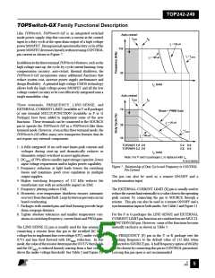
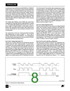
When a fault condition such as an open loop or shorted output
preventstheflowofanexternalcurrentintotheCONTROLpin,
the capacitor on the CONTROL pin discharges towards 4.8 V.
At 4.8 V, auto-restart is activated which turns the output
MOSFET off and puts the control circuitry in a low current
standby mode. The high-voltage current source turns on and
charges the external capacitance again. A hysteretic internal
supply under-voltage comparator keeps VC within a window of
typically4.8to5.8Vbyturningthehigh-voltagecurrentsource
on and off as shown in Figure 8. The auto-restart circuit has a
divide-by-8 counter which prevents the output MOSFET from
turningonagainuntileightdischarge/chargecycleshaveelapsed.
This is accomplished by enabling the output MOSFET only
when the divide-by-8 counter reaches full count (S7). The
counter effectively limits TOPSwitch-GX power dissipation by
reducing the auto-restart duty cycle to typically 4%. Auto-
restart mode continues until output voltage regulation is again
achieved through closure of the feedback loop.
When rectified DC high voltage is applied to the DRAIN pin
duringstart-up,theMOSFETisinitiallyoff,andtheCONTROL
pincapacitorischargedthroughaswitchedhighvoltagecurrent
sourceconnectedinternallybetweentheDRAINandCONTROL
pins. When the CONTROL pin voltage VC reaches
approximately 5.8 V, the control circuitry is activated and the
soft-start begins. The soft-start circuit gradually increases the
duty cycle of the MOSFET from zero to the maximum value
over approximately 10 ms. If no external feedback/supply
currentisfedintotheCONTROLpinbytheendofthesoft-start,
thehighvoltagecurrentsourceisturnedoffandtheCONTROL
pin will start discharging in response to the supply current
drawn by the control circuitry. If the power supply is designed
properly, and no fault condition such as open loop or shorted
output exists, the feedback loop will close, providing external
CONTROL pin current, before the CONTROL pin voltage has
had a chance to discharge to the lower threshold voltage of
approximately 4.8 V (internal supply under-voltage lockout
threshold). When the externally fed current charges the
CONTROL pin to the shunt regulator voltage of 5.8 V, current
Oscillator and Switching Frequency
Theinternaloscillatorlinearlychargesanddischargesaninternal
capacitance between two voltage levels to create a sawtooth
VUV
VLINE
0 V
S0
S0
S7
S1
S2
S6
S7 S0
S1
S2
S6
S7
S1 S2
S6
S7
S7
5.8 V
4.8 V
VC
0 V
VDRAIN
0 V
VOUT
0 V
1
2
3
2
4
Note: S0 through S7 are the output states of the auto-restart counter
PI-2545-082299
Figure 8. Typical Waveforms for (1) Power Up (2) Normal Operation (3) Auto-restart (4) Power Down.
E
7/01
August 8, 2000
6

 POWERINT [ Power Integrations ]