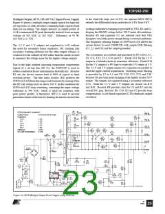
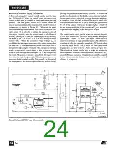
TOP242-250
TOPSwitch-GX
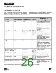
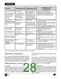
Function
Figures
TOPSwitch-II TOPSwitch-GX
Advantages
Switching Frequency N/A*
Option (Y, R and F
Packages)
66 kHz ±7%
14,15
• Lower losses when using RC and
RCD snubber for noise reduction
in video applications
• Allows for higher efficiency in
standby mode
• Lower EMI (second harmonic
below 150 kHz)
Frequency Jitter
N/A*
±4 kHz @ 132 kHz
±2 kHz @ 66 kHz
9,46
7
• Reduces conducted EMI
Frequency Reduction N/A*
At a duty cycle below
10%
• Zero load regulation without
dummy load
• Low power consumption at
no-load
Remote ON/OFF
N/A*
Single transistor or
11,22,23, • Fast ON/OFF (cycle-by-cycle)
optocoupler interface 24,25,26, • Active-on or active-off control
or manual switch
27,29,36, • Low consumption in remote off
37,38,39, state
40
• Active-on control for fail-safe
• Eliminates expensive in-line
on/off switch
• Allows processor controlled turn
on/off
• Permits shutdown/wake-up of
peripherals via LAN or parallel
port
Synchronization
N/A*
Single transistor or
optocoupler interface
• Synchronization to external lower
frequency signal
• Starts new switching cycle on
demand
Thermal Shutdown
125 °C min.
Latched
Hysteretic 130 °C
min. shutdown (with
75 °C hysteresis)
• Automatic recovery from thermal
fault
• Large hysteresis prevents circuit
board overheating
Current Limit
Tolerance
±10% (@ 25 °C)
-8% (0 °C to
100 °C)
±7% (@ 25 °C)
-4% Typical
(0 °C to 100 °C)**
• 10% Higher power capability due
to tighter tolerance
DIP
0.037” / 0.94 mm
0.037” / 0.94 mm
0.046” / 1.17 mm
0.137” / 3.48 mm
0.137” / 3.48 mm
0.068” / 1.73 mm
0.113” / 2.87 mm
• Greater immunity to arcing as a
result of build-up of dust, debris
and other contaminants
DRAIN
Creepage
at Package
SMD
TO-220
DRAIN Creepage at 0.045” / 1.14 mm
PCB for Y, R and F
Packages
• Performed leads accommodate
large creepage for PCB layout
• Easier to meet Safety (UL/VDE)
(R and F Package (performed leads)
N/A*)
Table 4 (cont). Comparison Between TOPSwitch-II and TOPSwitch-GX. *Not available **Current limit set to internal maximum
M
12/04
27

 POWERINT [ Power Integrations ]