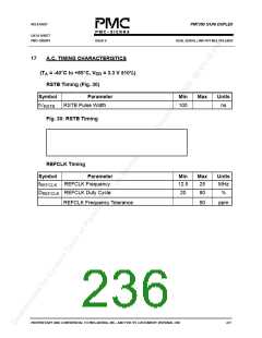
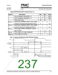
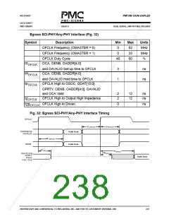
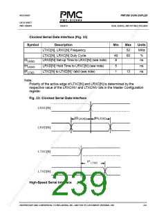
RELEASED
PM7350 S/UNI DUPLEX
DATA SHEET
PMC-1980581
ISSUE 8
DUAL SERIAL LINK PHY MULTIPLEXER
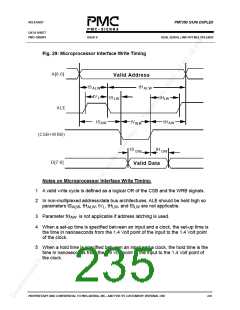
Fig. 29: Microprocessor Interface Write Timing
A[6:0]
Valid Address
tS
tH
ALW
ALW
tV
L
tS
tH
LW
LW
ALE
tS
tV
tS
tH
AW
AW
WR
(CSB+W RB)
tH
DW
DW
D[7:0]
Valid Data
Notes on Microprocessor Interface Write Timing:
1 A valid write cycle is defined as a logical OR of the CSB and the WRB signals.
2 In non-multiplexed address/data bus architectures, ALE should be held high so
parameters tS
, tH , tV , tH , and tS are not applicable.
ALW L LW LW
ALW
3 Parameter tH
is not applicable if address latching is used.
AW
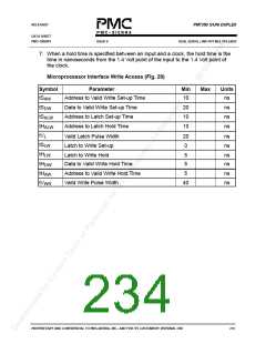
4 When a set-up time is specified between an input and a clock, the set-up time is
the time in nanoseconds from the 1.4 Volt point of the input to the 1.4 Volt point
of the clock.
5 When a hold time is specified between an input and a clock, the hold time is the
time in nanoseconds from the 1.4 Volt point of the input to the 1.4 Volt point of
the clock.
PROPRIETARY AND CONFIDENTIAL TO PMC-SIERRA, INC., AND FOR ITS CUSTOMERS’ INTERNAL USE
220

 PMC [ PMC-SIERRA, INC ]