RELEASED
PM7350 S/UNI DUPLEX
DATA SHEET
PMC-1980581
ISSUE 8
DUAL SERIAL LINK PHY MULTIPLEXER
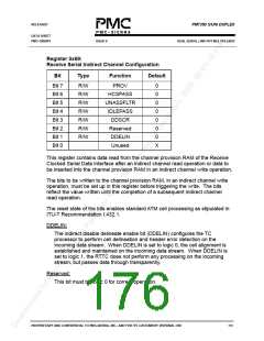
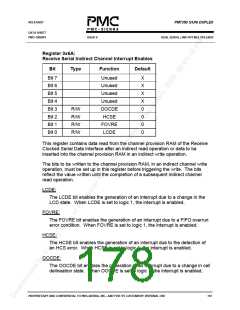
Register 0x6A:
Receive Serial Indirect Channel Interrupt Enables
Bit
Type
Function
Default
Bit 7
Bit 6
Bit 5
Bit 4
Bit 3
Bit 2
Bit 1
Bit 0
Unused
Unused
Unused
Unused
OOCDE
HCSE
X
X
X
X
0
0
0
0
R/W
R/W
R/W
R/W
FOVRE
LCDE
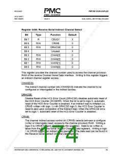
This register contains data read from the channel provision RAM of the Receive
Clocked Serial Data Interface after an indirect read operation or data to be
inserted into the channel provision RAM in an indirect write operation.
The bits to be written to the channel provision RAM, in an indirect channel write
operation, must be set up in this register before triggering the write. The bits
reflect the value written until the completion of a subsequent indirect channel
read operation.
LCDE:
The LCDE bit enables the generation of an interrupt due to a change in the
LCD state. When LCDE is set to logic 1, the interrupt is enabled.
FOVRE:
The FOVRE bit enables the generation of an interrupt due to a FIFO overrun
error condition. When FOVRE is set to logic 1, the interrupt is enabled.
HCSE:
The HCSE bit enables the generation of an interrupt due to the detection of
an HCS error. When HCSE is set to logic 1, the interrupt is enabled.
OOCDE:
The OOCDE bit enables the generation of an interrupt due to a change in cell
delineation state. When OOCDE is set to logic 1, the interrupt is enabled.
PROPRIETARY AND CONFIDENTIAL TO PMC-SIERRA, INC., AND FOR ITS CUSTOMERS’ INTERNAL USE
163

 PMC [ PMC-SIERRA, INC ]