PM73121ꢀAAL1gator II
Data Sheet
PMC-Sierra, Inc.
PMC-980620
,VVXHꢀꢁ
AAL1 SAR Processor
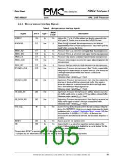
4.3.4 Microprocessor Interface Signals
Table 9. Microprocessor Interface Signals
Reset
Value*
Signal
ADDR17
Pin #
Type**
Description
216
In
NA
Address Bit 17 is bit 17 of the address bus directly connected to the
AAL1gator II. This bit is set to access the CMD_REG word.
HOLDOFF
172
Out
0
When Holdoff is asserted, the microprocessor cycle is delayed.
Implementations that have fast microprocessors may want to poll this
signal before accessing the device.
/PROC_RD
/PROC_WR
/PROC_CS
/PROC_ACK
177
176
175
174
In
In
NA
NA
NA
1
Processor Read is an active low read signal from the microprocessor.
Processor Write is an active low write signal from the microprocessor.
Processor Chip Select is a memory request from the microprocessor.
In
Out
Processor Acknowledge is an active low signal acknowledgment to the
microprocessor.
PROC_INT
173
178
Out
Out
0
1
Processor Interrupt is an active high interrupt to the microprocessor.
SP_DATA_CLK
Supervisory Processor (microprocessor) Read Clock is a signal with a
rising edge that causes memory or register read data to be written into
a 646-type external data buffer from which it is read by the
microprocessor.
Maximum output current (IMAX) = 8 mA.
SP_DATA_DIR
185
Out
1
Supervisory Processor (microprocessor) Data Direction controls the
direction of data in a 646-type external data buffer. This signal is
driven low when data is directed toward the device and high when
data is directed toward the microprocessor.
Maximum output current (IMAX) = 8 mA.
/SP_ADD_EN
/SP_DATA_EN
SYS_CLK
186
187
89
Out
Out
In
1
1
Supervisory Processor (microprocessor) Address Enable is an active
low buffer enable strobe to enable a 244-type address external buffer.
Maximum output current (IMAX) = 8 mA.
Supervisory Processor (microprocessor) Data Enable is an active low
buffer enable signal to enable a 646-type external data buffer.
Maximum output current (IMAX) = 8 mA.
NA
System Clock is the local clock used by the state machines within the
device. For SRTS T1/E1 clock recovery applications using the digital
synthesizer (refer to section 8 “Application Notes” on page 168), this
clock should be 38.88 MHz (155.52 MHz ÷ 4), but need not
necessarily be derived from the network. The maximum frequency is
40 MHz.
/RESET
/OE
183
184
In
In
NA
NA
Reset is an active low hardware reset.
Output Enable is an active low signal that enables outputs of the
device. It allows outputs to be disabled for in-circuit testing. Tie this
signal to ground for normal operation.
*Present when /RESET is asserted and SYS_CLK is being clocked.
**All input (In) and bidirectional (Bi) signals are pulled up through a large, internal pull-up resistor.
ꢇꢇ

 PMC [ PMC-SIERRA, INC ]