February, 2007
Switch Device Number Assignment Example
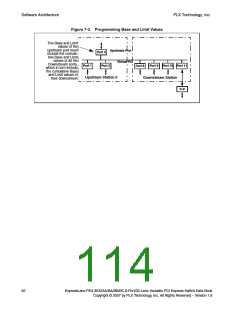
7.3.1.2
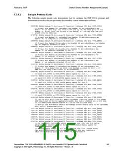
Sample Pseudo Code
The following sample pseudo code demonstrates how to configure the PEX 8532’s upstream and
downstream ports after they are previously discovered by system enumeration software.
CFGTYPE0 Write busnum 01,devicenum 00 function 0 address 18h data 0009_0201h
// Primary Bus Number 01, secondary Bus Number 02 and subordinate Bus
Number 09. At this step, the virtual PCI bus in the PEX 8532 gets the Bus
Number 02. After this, any access to Bus Number 02 from the upstream port
would refer to this bus.
CFGTYPE1 Write busnum 02,devicenum 01 function 0 address 18h data 0003_0302h
// Primary Bus Number 02, secondary Bus Number 03 and subordinate Bus
Number 03. an endpoint is attached to Port 1.
CFGTYPE1 Write busnum 02,devicenum 02 function 0 address 18h data 0004_0402h
// Primary Bus Number 02,secondary Bus Number 04 and subordinate Bus Number
04. an endpoint attached to Port 2.
CFGTYPE1 Write busnum 02,devicenum 08 function 0 address 18h data 0005_0502h
// Primary Bus Number 02,secondary Bus Number 05 and subordinate Bus
Number 05. an endpoint attached to Port 8.
CFGTYPE1 Write busnum 02,devicenum 09 function 0 address 18h data 0006_0602h
// Primary Bus Number 02,secondary Bus Number 06 and subordinate Bus
Number 06. an endpoint attached to Port 9.
CFGTYPE1 Write busnum 02,devicenum 10 function 0 address 18h data 0007_0702h
// Primary Bus Number 02,secondary Bus Number 07 and subordinate Bus
Number 07. an endpoint attached to Port 10.
CFGTYPE1 Write busnum 02,devicenum 11 function 0 address 18h data 0008_0802h
// Primary Bus Number 02,secondary Bus Number 08 and subordinate Bus
Number 09. This means that we have a P2P bridge attached to Port 11 of
PEX 8532 and only 1 more level of PCI hierarchy.
CFGTYPE1 Write busnum 02,devicenum 01 function 0 address 20h data 02FF_0200h
// need 0200_0000h to 02FF_FFFFh memory space for Port 1.
CFGTYPE1 Write busnum 02,devicenum 02 function 0 address 20h data 03FF_0300h
// need 0300_0000 to 03FF_FFFFh memory space for Port 2.
CFGTYPE1 Write busnum 02,devicenum 08 function 0 address 20h data 04FF_0400h
// need 0400_0000h to 04FF_FFFFh memory space for Port 8.
CFGTYPE1 Write busnum 02,devicenum 09 function 0 address 20h data 05FF_0500h
// need 0500_0000h to 05FF_FFFFh memory space for Port 9.
CFGTYPE1 Write busnum 02,devicenum 10 function 0 address 20h data 06FF_0600h
// need 0600_0000h to 06FF_FFFFh memory space for Port 10.
CFGTYPE1 Write busnum 02,devicenum 11 function 0 address 20h data 07FF_0700h
// need 0700_0000h to 07FF_FFFFh memory space for Port 11.
CFGTYPE0 Write busnum 01,devicenum 00 function 0 address 20h data 07FF_0200h
// the PEX 8532 will claim all Memory accesses from 0200_0000h to 07FF_FFFFh
and would send it to the appropriate port. Any memory address not within any
of the downstream Address spaces will go to the upstream port.
// Now set the Bus Master Enable and Memory Access Enable bits on the upstream
port and all downstream ports.
CFGTYPE0 Write busnum 01,devicenum 00 function 0 address 04h data 0000_0006h
CFGTYPE1 Write busnum 02,devicenum 01 function 0 address 04h data 0000_0006h
CFGTYPE1 Write busnum 02,devicenum 02 function 0 address 04h data 0000_0006h
CFGTYPE1 Write busnum 02,devicenum 08 function 0 address 04h data 0000_0006h
CFGTYPE1 Write busnum 02,devicenum 09 function 0 address 04h data 0000_0006h
CFGTYPE1 Write busnum 02,devicenum 10 function 0 address 04h data 0000_0006h
CFGTYPE1 Write busnum 02,devicenum 11 function 0 address 04h data 0000_0006h
// For each port configured above, registers 24h, 28h, and 2Ch can be
programmed to enable a 64-bit device Prefetchable Memory space for
downstream devices.
// Memory-Mapped access of all configuration registers listed above
can also be performed by programming the BAR0 and BAR1 registers
(for 64-bit Memory spaces) for busnum 01, devicenum 00.
ExpressLane PEX 8532AA/BA/BB/BC 8-Port/32-Lane Versatile PCI Express Switch Data Book
Copyright © 2007 by PLX Technology, Inc. All Rights Reserved – Version 1.6
93

 PLX [ PLX TECHNOLOGY ]