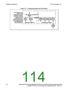
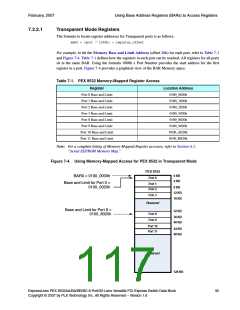
February, 2007
Switch Device Number Assignment Example
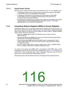
7.3.1.1
Configuration Register Programming Sequence
Registers that are defined by PCI-SIG Specifications can be accessed by Configuration mechanisms or
Memory command; device-specific registers can be accessed by Memory command, but not by
Configuration mechanisms (except for limited, indirect access through the NT Port Cursor Mechanism
Control Registers, when Non-Transparent mode is enabled).
Upstream port Base Address 0 and Base Address 1 registers (BAR0 and BAR1, offsets 10h and 14h,
respectively) map internal registers for Memory-Mapped I/O access. BAR0, is a 128-KB,
Non-Prefetchable BAR [the Prefetchable bit (bit 3) with default value 0 is not programmable]. Because
BAR0 maps to Non-Prefetchable Address space and the Address space is relatively small, it is
recommended that BAR0 be configured as a 32-bit BAR (default, with bits [2:1]=00b), rather than as a
64-bit BAR, to be mapped below the 4-GB Address Boundary space.
With BAR0 configured as a 32-bit BAR, BAR1 (which contains the upper 32 bits of address if BAR0 is
configured as a 64-bit BAR) must remain the default value 0h. If BAR0 is configured as a 64-bit BAR
and the BAR1 value is 0h, a 64-bit access to BAR0/1 returns an Unsupported Request (UR) error.
BAR0 and BAR1 can be disabled by setting the Ingress Control register Disable Upstream Port BAR0
and BAR1 Registers bit (Ports 0 and 8, offset 660h[25]). (Note: This feature is not available in Silicon
Revision AA.)
Register access must be 1 DWord (Byte Enables can select individual bytes). If a Memory Read requests
more than 1 DWord, the PEX 8532 returns the first DWord, with a Completion status of Completer
Abort. This error is flagged in the upstream port Device Status register (offset 70h) and Uncorrectable
Error Status register Completer Abort Status bit (offset FB8h[15]).
To program access to internal registers:
1. Program the Bus Number register in the upstream port (offset 18h).
2. Program the Bus Number registers in all downstream ports (offset 18h).
3. Program the Memory Base and Limit Address register (offset 20h) in all downstream ports.
4. Program BAR0/1 on the upstream port. (Optional, but necessary for Memory-Mapped access
to internal registers.)
5. Program the Memory Base and Limit Address register (offset 20h) in the upstream port, ensuring
the values claim all the space requested by all downstream ports.
6. Program the Command register Bus Master Enable and Memory Access Enable bits on all ports
(offset 04h[2:1], respectively).
ExpressLane PEX 8532AA/BA/BB/BC 8-Port/32-Lane Versatile PCI Express Switch Data Book
Copyright © 2007 by PLX Technology, Inc. All Rights Reserved – Version 1.6
91

 PLX [ PLX TECHNOLOGY ]