Software Architecture
PLX Technology, Inc.
7.3.1.3
Sample Packet Transfer
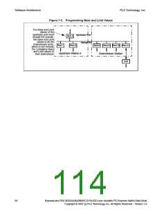
When all ports are configured using the sample code provided in Section 7.3.1.2, the following occurs:
• 32-bit Memory transactions from the upstream port, destined between addresses 0200_0000h
to 07FF_FFFFh, advance to the appropriate downstream port
• 32-bit Memory transactions from a downstream port, between addresses 0200_0000h
to 07FF_FFFFh, advance to the appropriate downstream port (if the transactions are
not within the Base-Limit range of that port)
• Transactions from a downstream port, outside the range of addresses 0200_0000h to 07FF_FFFFh
and outside PEX 8532 Memory-Mapped Register space (refer to Section 7.3.2 for details
regarding Register space), advance to the upstream port
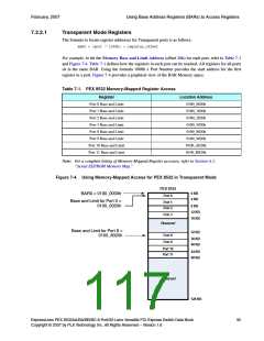
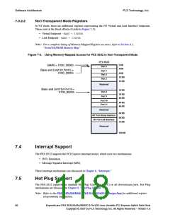
7.3.2
Using Base Address Registers (BARs) to Access Registers
Configuration requests can access only those registers that are defined by the PCI Express Base r1.0a.
These registers and the Device-Specific registers can all be accessed by Memory requests that target the
Memory space defined by the upstream port Base Address 0 and Base Address 1 (BAR0 and BAR1)
registers (offsets 10h and 14h, respectively).
• Upstream port BAR0 register requests 128-KB Memory space set aside for internal
PEX 8532 registers.
• Optionally, the upstream port BAR1 register can be used to place this internal register Memory
space anywhere in 64-bit System Memory space.
• After the upstream port BAR0 (and optionally, BAR1) register is programmed, all register
locations inside the PEX 8532 can be accessed from any port, using either Memory requests
or Configuration requests.
• Each port consumes 4 KB of Memory space for internal registers. Port 0 is at 0000h to 0FFFh,
Port 1 is at 1000h to 1FFFh, Port 8 is at 8000h to 8FFFh, and so forth.
For example, if the upstream port BAR0 register is programmed to 0100_0000h (using a Type 0
Configuration transaction) and the upstream port Command register Memory Access Enable bit is set
(offset 04h[1]=1; again, programmed using a Type 0 Configuration transaction), then all PEX 8532
registers can be accessed using Memory-Mapped Register accesses.
The following sections describe information specific to Transparent and Non-Transparent modes.
94
ExpressLane PEX 8532AA/BA/BB/BC 8-Port/32-Lane Versatile PCI Express Switch Data Book
Copyright © 2007 by PLX Technology, Inc. All Rights Reserved – Version 1.6

 PLX [ PLX TECHNOLOGY ]