Philips Semiconductors
Preliminary specification
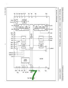
Stereo audio codec with SPDIF interface
UDA1355H
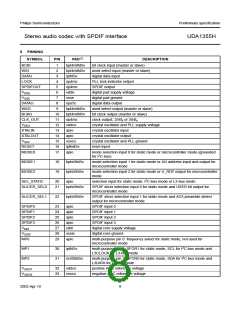
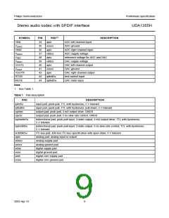
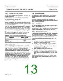
SYMBOL
VINL
PIN
PAD(1)
apio
DESCRIPTION
34
35
36
37
38
39
40
41
42
43
44
ADC left channel input
ADC ground
VSSA2
VINR
vssco
apio
ADC right channel input
ADC supply voltage
VDDA2
VREF
vddco
apio
reference voltage for ADC and DAC
DAC supply voltage
DAC left channel output
DAC ground
VDDA1
VOUTL
VSSA1
VOUTR
RTCB
MUTE
vddco
apio
vssco
apio
DAC right channel output
test control input
ipthdt5v
iipthdt5v
DAC mute input
Note
1. See Table 1.
Table 1 Pad description
PAD
DESCRIPTION
iptht5v
input pad; push-pull; TTL with hysteresis; 5 V tolerant
input pad; push-pull; TTL with hysteresis; pull-down; 5 V tolerant
output pad; push-pull; 4 mA output drive; CMOS
ipthdt5v
op4mc
ops5c
output pad; push-pull; 5 ns slew rate control; CMOS
bpt4mtht5v
bidirectional pad; push-pull input; 3-state output; 4 mA output drive; TTL with hysteresis;
5 V tolerant
bpts5tht5v
bidirectional pad; push-pull input; 3-state output; 5 ns slew rate control; TTL with hysteresis;
5 V tolerant
iic400kt5v
apio
I2C-bus pad; 400 kHz I2C-bus specification with open drain; 5 V tolerant
analog pad; analog input or output
analog supply pad
vddco
vssco
vdde
analog ground pad
digital supply pad
vsse
digital ground pad
vddi
digital core supply pad
vssis
digital core ground pad
2003 Apr 10
9

 NXP [ NXP ]