Philips Semiconductors
Preliminary specification
Fault-tolerant CAN transceiver
TJA1054
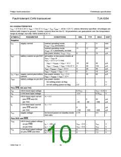
DC CHARACTERISTICS
VCC = 4.75 to 5.25 V; VBAT = 5 to 27 V; VSTB = VCC; Tamb = −40 to +125 °C; unless otherwise specified. All voltages are
defined with respect to ground. Positive currents flow into the IC. All parameters are guaranteed over the temperature
range by design, but only 100% tested at 25 °C.
SYMBOL
PARAMETER
CONDITIONS
MIN.
TYP.
MAX.
UNIT
Supplies
ICC
supply current
normal operating mode;
VTXD = VCC (recessive)
4
7
11
mA
mA
µA
normal operating mode;
VTXD = 0 V (dominant); no load
11
0
17
0
27
10
low power modes; VTXD = VCC
IBAT
battery current on pin BAT all modes; in low power modes at
VRTL = VBAT or
VRTL < 2.5 V (>1.5 ms)
V
BAT = VWAKE = VINH = 12 V
10
5
30
30
20
0
50
125
30
µA
µA
µA
µA
µA
VBAT = VWAKE = VINH = 5 to 27 V
BAT =VWAKE = VINH = 3.5 V
BAT = VWAKE = VINH = 1 V
V
V
5
0
10
I
CC + IBAT supply current plus battery low power modes; VCC = 5 V;
current VBAT = VWAKE = VINH = 12 V
battery voltage on pin BAT low power modes
for setting power-on flag
for not setting power-on flag
−
35
60
VBAT
−
−
−
1
V
V
3.5
−
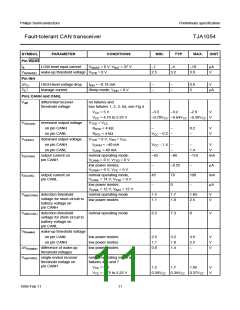
Pins STB, EN and TXD
VIH
VIL
IIH
HIGH-level input voltage
0.7VCC
−
−
VCC + 0.3 V
LOW-level input voltage
HIGH-level input current
pins STB and EN
pin TXD
−0.3
0.3VCC
V
VI = 4 V
−
9
20
µA
µA
−25
−80
−200
IIL
LOW-level input current
pins STB and EN
pin TXD
VI = 1 V
4
8
−
µA
µA
V
−100
−320
−800
4.5
VCC
supply voltage
for forced power-on standby mode 2.75
(fail safe)
−
Pins RXD and ERR
VOH HIGH-level output voltage
on pin ERR
on pin RXD
lO = −100 µA
IO = −1 mA
V
V
0
0
CC − 0.9 −
VCC
VCC
0.4
V
V
V
V
CC − 0.9 −
VOL
LOW-level output voltage IO = 1.6 mA
on pins ERR and RXD
−
−
IO = 7.5 mA
1.5
1999 Feb 11
10

 NXP [ NXP ]