Philips Semiconductors
Preliminary specification
Fault-tolerant CAN transceiver
TJA1054
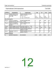
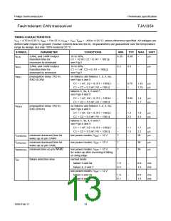
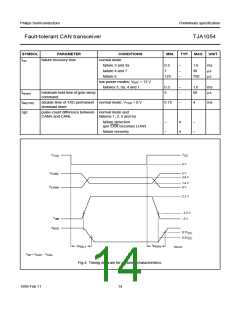
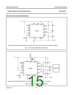
TIMING CHARACTERISTICS
VCC = 4.75 to 5.25 V; VBAT = 5 to 27 V; VSTB = VCC; Tamb = −40 to +125 °C; unless otherwise specified. All voltages are
defined with respect to ground. Positive currents flow into the IC. All parameters are guaranteed over the temperature
range by design, but only 100% tested at 25 °C.
SYMBOL
PARAMETER
CONDITIONS
MIN.
TYP. MAX. UNIT
tt(r-d)
CANL and CANH output
transition time for
10 to 90%;
C1 = 10 nF; C2 = 0; R1 = 100 Ω;
0.35
0.60
−
µs
recessive-to-dominant
see Fig.5
tt(d-r)
CANL and CANH output
transition time for
dominant-to-recessive
10 to 90%;
C1 = 1 nF; C2 = 0; R1 = 100 Ω;
see Fig.5
0.2
0.3
−
µs
tPD(L)
propagation delay TXD to
RXD (LOW)
no failures and failures 1, 2, 5, 6a;
see Figs 4 and 5
C1 = 1 nF; C2 = 0; R1 = 100 Ω
C1 = C2 = 3.3 nF; R1 = 100 Ω
−
−
0.75
1
1.35
1.75
µs
µs
failures 3, 3a, 4, 6 and 7;
see Figs 4 and 5
C1 = 1 nF; C2 = 0; R1 = 100 Ω
C1 = C2 = 3.3 nF; R1 = 100 Ω
−
−
0.85
1.1
1.4
1.7
µs
µs
tPD(H)
propagation delay TXD to
RXD (HIGH)
no failures and failures 1, 2, 5, 6a;
see Figs 4 and 5
C1 = 1 nF; C2 = 0; R1 = 100 Ω
C1 = C2 = 3.3 nF; R1 = 100 Ω
−
−
1.2
2.5
1.9
3.3
µs
µs
failures 3, 3a, 4, 6 and 7;
see Figs 4 and 5
C1 = 1 nF; C2 = 0; R1 = 100 Ω
C1 = C2 = 3.3 nF; R1 = 100 Ω
low power modes; VBAT = 12 V
−
−
7
1.1
1.5
−
1.7
2.2
38
µs
µs
µs
tCANH(min) minimum dominant time for
wake-up on pin CANH
tCANL(min) minimum dominant time for
wake-up on pin CANL
low power modes; VBAT = 12 V
7
7
−
−
38
38
µs
µs
tWAKE(min) minimum time on pin WAKE
low power modes; VBAT = 12 V;
for wake-up after receiving a falling
or rising edge
tdet
failure detection time
normal mode
failure 3 and 3a
1.6
0.3
−
−
8.0
1.6
ms
ms
failure 4, 6 and 7
low power modes; VBAT = 12 V
failure 3 and 3a
1.6
0.1
−
−
8.0
1.6
ms
ms
failure 4 and 7
1999 Feb 11
13

 NXP [ NXP ]